You design the future. We help you make it happen.
Products
Displaying 397 - 408 of 902

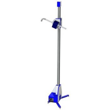
SOLEVAACC01PAK*
Matrox Solios Accessory Kit for SOL2MEVCLB* and SOL2MEVCLF*
Includes One Panel Mount DB-9 Based Trigger Cable and Full-Height Bracket
Quick Ship Inventory is available
Boresite -18.5° to +45°
Height range 1.0 - 4.0m
Pneumatic polarization change 90°
Electric stepper motor height
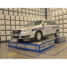
3,000kg capacity
Adjustable axle length and width
120k/hr max speed dynamometer
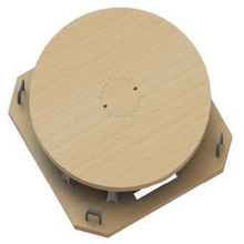
Free-standing turntable for anechoic Chambers.
Diameter 1.2 m
Load capability 300 kg
Height 140 mm
Other diameters and load capabilities are available on request.
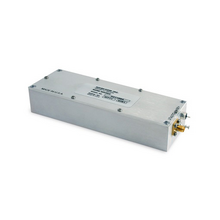
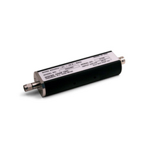
AWGN as high as +13 dBm
Bandwidths up to 18 GHz
Bandwidth, output power, and flatness can be modified for specific applications
TTL controlled attenuation
The NC1000 Series amplified noise modules produce AWGN as high as +13 dBm, and have bandwidths up to 18 GHz. The high power modules are designed to test noise immunity for Cable TV equipment, secure communication channels, and military jamming systems. The lower power modules, <= 0 dBm, are random jitter sources for many applications including, PCIexpress, Infiniband, and 10 GigE. The Bandwidth, output power, and flatness can be modified for specific applications. A newly developed TTL controlled attenuation feature is also available.
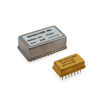
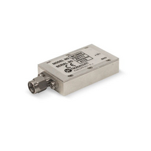
High-level noise modules mounted on a circuit board
Modified BW, output power, and flatness specifications
The NC2000 Series amplified noise modules are an excellent choice for high-level noise modules mounted on a circuit board. The NC2000 Series modules are housed in 24, or14-pin dual-inline packages. The NC4000 series modules are housed in a 40-pin module that cover similar noise bands to the NC2000, but have higher crest factor, and 60 dB of TTL controlled attenuation. Modified BW, output power, and flatness specifications are available for these modules. Please consult Noisecom for availability, and appropriate package style.
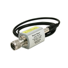
The overall performance of a power meter dependents on the power sensor employed. Maury has a variety of quality power sensors to meet virtually all applications. Maury has a complete line of Peak and Average power sensors up to 40 GHz for all of your fast rise time, wide bandwidth and wide dynamic range applications. In this document, browse through our large variety of advanced sensor solutions.
Excellent temperature and voltage stability
Units for noise figure meters feature 15.5-dB ± 0.75 dB ENR output
High-output units for radar and satellite communications system testing feature output between 26 and 35 dB ± 1 dB ENR
Ideal for applications requiring high ENR and immunity to large incident RF power
Low VSWR
Built-in isolator
The NC3400 Series coaxial AWGN noise sources are an excellent choice for applications requiring high ENR and immunity to large incident RF power, such as ATE, radiometer, and radar systems. The calibration accuracy and flatness of the NC3400 Series noise sources are enhanced by their low VSWR. The built-in isolator provides almost constant output impedance as the noise source bias is switched on and off. The isolator also protects the noise diode from incident RF power (consult the factory for higherpower units).
Broadband coverage
Extremely good temperature stability
Superior voltage stability
Noise figure meter-compatible
The NC346 Series is designed for precision noise figure measurement applications. Each module’s low VSWR reduces multiple reflections and significantly increases the measurement accuracy for most noise figure test configurations.
High ENR
Wide frequency range
Custom frequencies available
The NC3600 Series coaxial noise sources are an excellent choice for applications requiring high ENR, such as ATE, radiometer, and radar systems.
An SMA male connector is standard for the RF output and feed thrus for bias input. SMA female is an option. Custom frequencies and flatness available. Contact the factory with your request.
Outstanding stability
Fast switching speed
Ripple-free response over standard waveguide bands
The NC5000A Series AWGN noise sources feature outstanding stability, switching speed, and ripple-free response over standard waveguide bands. The high stability of the NC5000A Series allows these units to be used in place of cumbersome gas tube noise sources.
Ripple in the output of noise sources has a direct effect on measurement accuracy, so Noisecom has tailored the response of the NC5000A Series so that ripple is minimized throughout the specified frequency range.