You design the future. We help you make it happen.
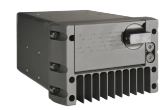
FormFactor - Cascade High Current Probe - Test power devices on wafer with high-performance and low-contact resistance on smaller pads
- Enables wafer probing up to 100 A pulsed and 10A DC
- Innovative multi-fingertip design provides even distribution of current
- Supports up to 500 V
- Replaceable Tungsten probe tips
- Temperature range of -60°C to 300°C
- Minimal contact resistance at the pad-tip junction to reduce heating during measurements, with fewer probe marks
- Prevents against thermal runaway
- Measure devices on wafer at higher currents than ever before
- Small scrub minimizes damage to aluminum pad
- Small footprint – tip fits on a 1 mm pad
Designed specifically for testing power devices on wafer, the HCP probe reduces probe and device destruction at high currents by minimizing contact resistance at the wafer-to-probe interface to prevent device heating at the tip. The innovative multi-finger design distributes the current over multiple contact points at the tip and is joined by a single heatsink which pulls heat from the probe tip.
More Product Information
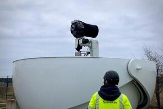
- Multi-Missions and Applications: Earth Observation (EO), high throughput bi-directional telecommunication, feeder link or Deep Space
- 100% Safran In-House Solution: Compatible with SDA, CCSDS and HPE standards
- Communication Data Rates: 10 to 100 times higher thanks to Cortex Lasercom

- High performance power bypassing provides low-impedance and resonant-free connections to 20 GHz
- RF bandwidth to 500 MHz
- Long probe life: > 250,000 contacts
- Beryllium-copper tips for gold pads or tungsten for aluminum pads
- Oscillation-free testing of wide-bandwidth analog circuits
- Use with ACP series probes to provide functional at-speed testing for known-good-die
- Mix multiple contact types: Ground, Power (Standard or Eye-Pass), Logic/Signal
- Low and repeatable contact resistance on aluminum pads ( < 0.25 Ω on Al, < 0.01 Ω on Au)

- Support for the highest speeds available in CoaXPress 2.0
- Connect to and capture from up to four cameras or combine connections for even higher data rates
- Simplify cabling with PoCXP support between cameras and vision computer
- Offload host computer of custom image processing using a field-programmable gate array (FPGA) device
- Distribute image processing workload across multiple computers through data forwarding capability
- Synchronize with sensors, encoders, and controllers with ample auxiliary I/Os for each CoaXPress connection
- Use license fingerprint for Aurora Imaging Library and avoid the need for a separate hardware key
- Monitor and troubleshoot acquisition performance in detail using Aurora Gecho event-logging tool
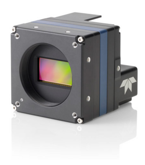
- Reduced dark noise levels and improved dark offset
- Improved sensitivity, including NIR response
- In-camera image pre-processing (lens shading correction, pixel correction)
- Large full well when using in-sensor binning >142Ke
- Thousands of frames per second in Partial Scan Mode (ROI)
- Multi-ROI support (up to 32 ROI) and Cycling Mode
- Advanced Sequencer functions of different features
- LTE/4G Mitigation: LTE/4G, WCS & Customized Rejection Filters (Upgradable During Antenna Lifetime)
- Easy Integration: Tri-Band even with Dishes as Small as 6’/1.8m
- SCM 1000 Hz Scan Rate: Highest Accuracy of Tracking
- No RF-Band Compromise: Concentric 3-Band Feed, without need of Dichroic Filter
- Modular L - S or C-Band: Simple Add-On upgrade without any Structural Change
- For cameras up to 40 x 40mm cross section
- Front tube for easy lens access
- Robust construction
- Compact size
- High IP protection class
- Flexible camera positioning
- High chemical resistance
- Vibration‐proof mounting
- Camera mount included
- Excellent heat dissipation
- File Server Capability: User-Defined Media Partitioning
- Qualified for Hard Environment: DO-160, MIL-STD-704, -461, -810
- Designed to Minimize Obsolescence Risk & Management: FPGA-Based Design
- High-Definition Video, Processing & Recording: VESA, HD-SD, DVI
- High-Capacity Rugged Removable Cartridge: 64TB to 2TB
- Databus: MIL-STD-1553B (MT/RT, ARINC429, RS422
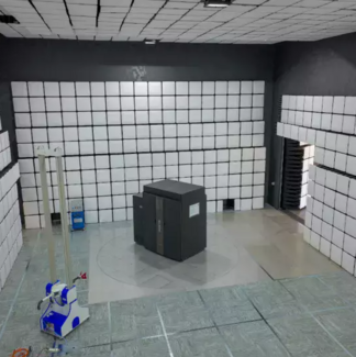
The Gold standard for EMC Anechoic Chambers, this 10 meter test range ensures EMC compliance testing Emission and Immunity testing and is compliant to ANSI C63.4/CISPR-16-1-4 with a Test Volume diameter of 4 meters or greater. The most versatile and accurate of EMC test chambers. Ferrite tiles and hybrid pyramidal absorbers allow for high accuracy and performance while meeting compact space requirements.
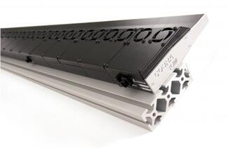
ProPhotonix designs and manufactures a wide range of LED Line Lights configurable to suit almost any application. All of our line lights offer high intensity illumination and excellent uniformity ensuring that the system performs consistently and reliably in even the most challenging of applications.
Our LED Line Lights are ideally suited to line scan and web inspection of a host of materials and products, including paper, foil, metal, road surfaces, PCBs and semiconductors.
FormFactor, Inc.
Website
FormFactor, Inc. (NASDAQ:FORM) is a leading provider of essential test and measurement technologies along the full IC life cycle – from characterization, modeling, reliability, and design de-bug, to qualification and production test.
We constantly strive to help our customers solve the advanced test and measurement challenges of the broader semiconductor industry. Our focus on customer partnership, innovation, agility and operational excellence allows us to earn sustainable business every day.
