You design the future. We help you make it happen.
Products
Displaying 373 - 384 of 902
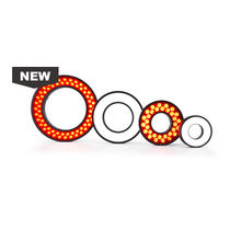
LUMIMAX® LED Ring Lights are ideal for the uniform illumination of flat, matte and reflective surfaces. A range of different sizes and performance classes of the LED ring light provide the optimum illumination for every application.
Lens exchange options, diffusers, Fresnel lenses and polarisation filters allow the optimisation of the radiation characteristic to the required inspection task – even at working distances of several meters. Calculate the optimal illumination area of the LR-series Ring Lights for your application easily and simply with the help of our practical tool.
Direct mounting on the camera or lens using optional accessories simplifies integration of the LED Ring Lights into Machine Vision systems.
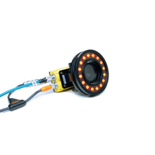
An extensive range of optical, electrical and mechanical accessories for LUMIMAX® LED Lights simplify both adaptation to customer-specific requirements and the connection to the machine environment. The innovative solutions allow for compact, fast and easy integration of LUMIMAX® LED Lights. This saves additional design and mounting work, which means that significant cost savings can be achieved.
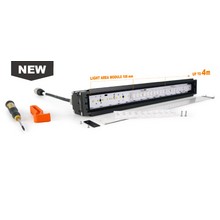
With the powerful modular LUMIMAX® LED Bar Lights test areas can be uniformly illuminated even from distances of more than 1 meter. The Bar Lights with integrated controller technology are available in different configurations for incident and backlight applications.
The modular bar lights expand the portfolio and include now bar lights of up to 4 meters for even larger test areas. Thanks to the modular concept, specific sizes can be realized quickly and without additional development costs. You can select standard versions using our product configurator. Please contact our sales team for special enquiries about customised lengths.
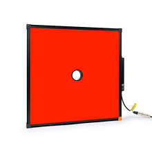
Large surface lighting with dimensions from 50 mm x 250 mm
Rectangular, square and elongated design in 50 x 50 mm light field modules freely definable depending on requirements
Lighting solution individually adapted to the application from the cost-optimized standard portfolio

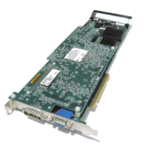
Mfg: Matrox
Model: DA5WINPU
Condition: Open Box
Description: Matrox Design Assistant 5 Flowchart-based Vision Software for Windows

Quantity in Stock: 1
Quick Ship Inventory is available

Quantity in Stock: 1
Quick Ship Inventory is available
Quantity in Stock: 1
Quick Ship Inventory is available
Quantity in Stock: 1
Quick Ship Inventory is available

Quantity in Stock: 1
Quick Ship Inventory is available
Quantity in Stock: 1
Quick Ship Inventory is available