You design the future. We help you make it happen.
FormFactor - Cascade ACP Probe – Cryo/Vacuum - Superior mechanical properties at cryogenic temperatures
-
Functional temperature range of -263 to +150°C
-
Stainless steel tip material for thermal decoupling
-
Coaxial cable with TCE matched inner and outer conductors
-
Consistent tip geometry even at cryogenic temperatures
Designed to provide superior mechanical properties at cryogenic temperatures while maintaining solid RF measurement performance. Functional temperature range of -263 to + 150 ° C. Consistent tip geometry even at cryogenic temperatures.
More Product Information

- Ultra-low, fA-level current and fF-level capacitance measurements from -65 °C to + 300 °C
- Guarantees fully-guarded measurements to fA and fF levels
- Individual connectors provide force-sense connection for quasi-Kelvin and CV measurements
- Allows probing of different pad materials and sizes
- Fast replacement of worn probes without the need for tools
Flexibility
- DC, AC and RF/microwave device characterization, 1/f, WLR, FA and design debug
- Full thermal range of -60°C to +300°C
- Compatible with TopHat or IceShield
- Usage of manual and motorized positioners, probe cards within EMI-shielded environment
- Upgrade path to meet your future needs
- Stable and repeatable measurements over a wide thermal range
High accuracy and repeatability
- Reliable and repeatable contact
- Moisture-free, light-tight and EMI-shielded test environment with MicroChamber® technology
- Advanced EMI-shielding with PureLine and AttoGuard technologies available
- Superior low-leakage and low-noise measurements
- Safe and accurate hands-off testing
- Minimizes settling times for efficient measurements over full thermal range
See "Specifications & Details" tab for more key features

- High-quality construction with low-noise electrical performance
- Kelvin version for convenient 4-point measurements
- Replaceable coaxial probe tips, with choice of tip radii, and full electrical guard to the probe tip
- SSMC 50 connectors
- Ultra-low, fA and fF measurements from -65 º C to 150 º C

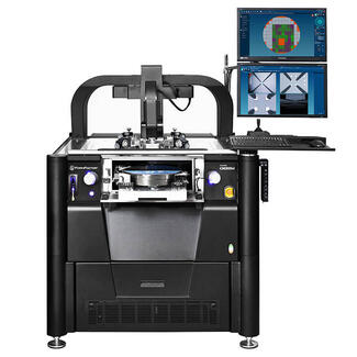
Comprehensive, Turn-key Integrated Measurement System (IMS) with Keysight PDA for On-wafer R&D Power Semiconductor Device Characterization Measurements

-
Ease of use – Less experienced operators can perform an RF calibration up to 500 GHz by simply pushing a button. This reduces the need of experienced users full time on each system.
-
Reduced Soak Time – The system will automatically re-align the probes to the pads if they drift from alignment. This reduces test time and increases throughput.
-
Unattended Use – Measurements can be left running over night or the weekend, testing all devices on the wafer, and at different temperatures without the need of an operator.
-
Calibration Monitor and Re-calibration – System will continuously monitor calibration drift, and automatically re-calibrate the system should the drift exceed a predefined limit.

Flexibility
- Ideal for a wide range of applications such as RF, mm-Wave and sub-THz characterization, FA, DWC, MEMS, optoelectronic tests and WL
- Re-configurable and upgradable as requirements grow
- Minimizes setup times with no loss in performance or accuracy
- Seamless integration of various measurement instruments
Stability
- Solid station frame
- Built-in vibration-isolation solution for superior vibration attenuation
- Rigid microscope bridge
- Compact and rigid mechanical design
- Highly accurate measurement results
- Incorporates best-known methods
Ease of Use
- Ergonomic and straightforward design for comfortable and easy operation
- Low-profile design
- Simple microscope operation
- Quick and ergonomic change of DUT through pull-out stage
- Minimize training efforts
- Fast time to data
- Convenient operation

- Probe loss is 3 dB typical between 140 and 200 GHz, S11/S22 15 dB typical
- Reduced unwanted couplings and transmission modes
- Able to shrink pad geometries to 25 x 35 µm (best case)
- Typical contact resistance < 0.05 Ω on Al, < 0.02 Ω on Au
- WR15, WR12, WR10, WR8, WR6, WR4, WR3, and WR2 bands available.

- Light-tight version and EMI-shielded version for low noise and light-sensitive measurements
- Application flexibility, ideal for use in high frequency applications
- Sized to accommodate thermal chucks, laser cutter, and video equipment on the probe system
- Suitable for integration with vibration isolating tables

Flexibility
- Different substrate carriers for wafers up to 200 mm or single dies
- Probe cards and/or up to eight positioners
- Use with liquid nitrogen or helium, depending on the target temperature. Or use of cryo-cooler for dry-cooling option.
- Accessories available, such as black bodies and optical motion analysis tools
- Optional upgrade for 300 mm wafer
- Designed for industrial environments
- Covers wide range of measurements (I-V, C-V, RF, MEMS, OPTO)
- Ideal for small structures
See "Specifications & Details" tab for more key features
FormFactor, Inc.
Website
FormFactor, Inc. (NASDAQ:FORM) is a leading provider of essential test and measurement technologies along the full IC life cycle – from characterization, modeling, reliability, and design de-bug, to qualification and production test.
We constantly strive to help our customers solve the advanced test and measurement challenges of the broader semiconductor industry. Our focus on customer partnership, innovation, agility and operational excellence allows us to earn sustainable business every day.

