You design the future. We help you make it happen.
Products
Displaying 433 - 444 of 902
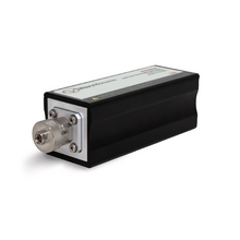
4 kHz to 6 GHz and 10 MHz to 6, 18, and 40 GHz power sensors
-60 dBm to +20 dBm dynamic range
Pulse, Average, CW and Modulation modes
True average measurements with essentially no modulation bandwidth limitations
Real-Time Power Processing™ technology for virtually no gaps in signal acquisition and zero measurement latency
100,000 measurements per second
Synchronized multi-channel measurements
Suite of advanced measurement and analysis software
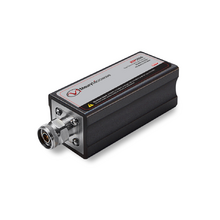
6 GHz, 8 GHz, 18 GHz and 40 GHz RF Power Sensors
Up to 195 MHz video bandwidth with 3 ns rise time
Real-Time Power ProcessingTM technology with zero measurement dead time
100,000 measurements per second
Power Analyzer Suite advanced measurement and analysis software
Crest factor, CCDF and statistical measurements
10 GS/s effective sample rate
100 MS/s continuous sample rate
Synchronized multi-channel measurements
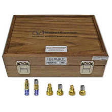
Directly compatible with most commercial VNA’s
Available as polynomial and characterized device kits
Measure S-Parameters with uncertainty when used in conjunction with Maury’s Insight software platform
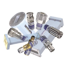
Maury offers coaxial and waveguide VNA calibration kits.
Calibration-grade metrology standards
Used for VNA calibration and/or calibration validation
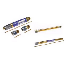
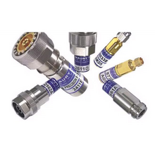
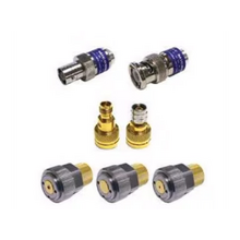
Coaxial air lines are air-dielectric transmission lines with highly accurate dimensions that can be used as fundamental impedance standards in measurement and calibration applications, and may also be used to establish reference positions for measurements.
Calibration-grade metrology standards
Used for VNA calibration and/or calibration validation
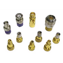
Calibration-grade metrology standards
Used for VNA calibration and/or calibration validation
Maury mismatch airlines have been designed as verification standards to be used in VNA calibration validation. Each mismatch airline is provided with factory S-parameters data that can be compared with user-measured S-parameters for VNA calibration validation. Measurement uncertainty is also provided, and uncertainty boundaries can be used for definitive calibration validation when used in conjunction with MT940B Insight Real-Time Uncertainty Add-On.
Calibration-grade metrology standards
Used for VNA calibration and/or calibration validation
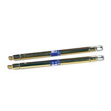
Precision standard mismatches are fixed coaxial terminations, which are used to introduce a known VSWR into a 50 ohm transmission system. These mismatches are extremely useful in a wide variety of applications and are quick and easy to use. They can be used to calibrate swept reflectometers, verify network analyzer calibration, establish impedance references in TDR measurements.
Calibration-grade metrology standards
Used for VNA calibration and/or calibration validation
Calibration-grade metrology standards
Used for VNA calibration and/or calibration validation
Fixed flush and fixed offset short circuit terminations (shorts) are used to establish reference planes in transmission systems and as key elements in the calibration of vector network analyzers (VNAs). Offset shorts can be used for banded calibrations of VNA. Those with the longest offset are often used to evaluate the calibration effectiveness of a VNA by measuring the effective source match after calibration.
Calibration-grade metrology standards
Used for VNA calibration and/or calibration validation
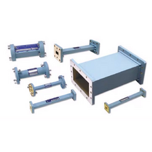
Precision waveguide sections are a useful component in the VNA calibration validation process, and can also be used as sample holders for material measurements.
Speed: Calibration is faster since there is no need to manually connect and disconnect standards.
Accuracy: Eliminates errors caused by manual handling, such as connector inconsistencies and improper torquing.
Ease of Use: Minimal user interaction is required, making calibration simpler and more accessible.
Reliability: Reduces wear and tear on VNA ports and connectors, prolonging their lifespan.
Consistency: Provides repeatable results across multiple calibration sessions and users.
S-parameters comparison of user-characterized and factory-characterized verification standards
S-parameters comparison of user-characterized and factory-characterized verification standards with measurement uncertainty boundaries
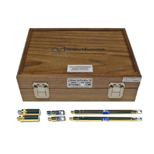
Includes beaded airline, mismatch airline, offset shorts and fixed loads