You design the future. We help you make it happen.
FormFactor - Cascade WPH Probe - Multi-contact DC probe with full-radius needles
- Full-radius, nickel-plated tungsten needles
- Power bypass inductance: 16 nH
- Supports collinear and non-standard needle configurations
- Support up to a maximum of 12 ceramic blades DC needles / contacts
- Ideal for probing the entire circuit for functional test
- DC probes can provide power or slow logic to circuit under test
The WPH probes feature up to 12 ceramic-bladed, nickel-plated, tungsten needles with a 2 x 12 square pin cable interface. The circuit board has been laid out such that both series and shunt components can be added to the signal path of each needle.
Document
Document
Document
More Product Information

-
Replace costly and inflexible test fixtures with easy-to-use probe tips
-
Long lifetime – typically over 1,000,000 contacts
-
GS/SG footprint up to 4 GHz and GSG up to 20 GHz
-
High-power RF test: up to 30 Watts
-
Test at temperatures from -60°C to 200°C

- Power bypass inductance: 8 nH
- Standard DCQ probes have flat tip needles available in nickel-plated tungsten or BeCu with diameters of 0.75 mil, 1.0 mil and 1.5 mil.
- Supports collinear and non-standard needle configurations
- Up to 16 DC for standard; maximum of 24 DC for custom
- Ideal for probing the entire circuit for functional test
- DC probes can provide power or slow logic to circuit under test

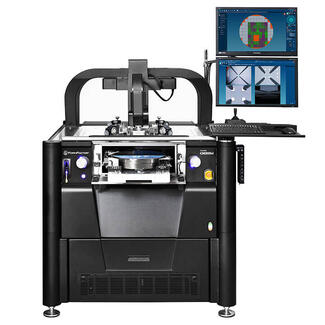
Environmental Control
- Wafer temp verified <4.5 K (with 44 RF probes in contact)
- Magnetic field suppression to <200 nT
- Highly uniform wafer temperature
- Precise thermal stability and control
- Solid construction with granite base enables precision motion and vibration control
See "Specifications & Details" tab for more key features

Flexibility
- Ideal for a wide range of applications such as RF, mm-Wave and sub-THz characterization, FA, DWC, MEMS, optoelectronic tests and WL
- Re-configurable and upgradable as requirements grow
- Minimizes setup times with no loss in performance or accuracy
- Seamless integration of various measurement instruments
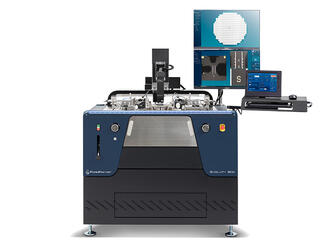
Stability
- Solid station frame
- Built-in vibration-isolation solution for superior vibration attenuation
- Rigid microscope bridge
- Compact and rigid mechanical design
- Highly accurate measurement results
- Incorporates best-known methods
Ease of Use
- Ergonomic and straightforward design for comfortable and easy operation
- Low-profile design
- Simple microscope operation
- Quick and ergonomic change of DUT through pull-out stage
- Minimize training efforts
- Fast time to data
- Convenient operation
Flexibility
- DC, AC and RF/microwave device characterization, 1/f, WLR, FA and design debug
- Full thermal range of -60°C to +300°C
- Compatible with TopHat or IceShield
- Usage of manual and motorized positioners, probe cards within EMI-shielded environment
- Upgrade path to meet your future needs
- Stable and repeatable measurements over a wide thermal range
High accuracy and repeatability
- Reliable and repeatable contact
- Moisture-free, light-tight and EMI-shielded test environment with MicroChamber® technology
- Advanced EMI-shielding with PureLine and AttoGuard technologies available
- Superior low-leakage and low-noise measurements
- Safe and accurate hands-off testing
- Minimizes settling times for efficient measurements over full thermal range
See "Specifications & Details" tab for more key features

- Light-tight version and EMI-shielded version for low noise and light-sensitive measurements
- Application flexibility, ideal for use in high frequency applications
- Sized to accommodate thermal chucks, laser cutter, and video equipment on the probe system
- Suitable for integration with vibration isolating tables
- Mechanical Platen Lift: Enhances safety during complex RF set-ups, increasing operator confidence and minimizing the risk of errors.
- Ease of Use and Advanced Automation: Fully compatible with FormFactor’s Autonomous RF and DC measurement assistants, as well as Velox Dash™ companion app control.
- Reconfigurable Platen Inserts: Quickly switch between TopHat, PCH, and IceShield inserts within minutes to support a wide variety of test configurations.
- Spacious Platen Design: Provides flexibility for both RF and DC setups without space limitations, ensuring easy integration of different configurations.
- Compact Design: Small footprint with field-upgradable components for smooth integration into existing test cells.
- Low-Volume MicroChamber and FemtoGuard Thermal Triaxial Chuck: Included by default

Flexibility
- Different substrate carriers for wafers up to 150 mm or single dies
- Up to six positioners
- Optional thermal chuck (-60°C to 300°C) and pressure regulation
- Probing with an open chamber lid possible under atmospheric condition
- Specially designed for laboratory environments
- Covers wide range of measurements (I-V, C-V, RF, MEMS, OPTO)
See "Specifications & Details" tab for more key features

SlimVue Microscope
- Combined eye-pieces and CCD camera mount
- 3x zoom and quick lens exchange
- Quick lens exchange
- 1 um optical resolution
- Minimized scope footprint
- Fast change from navigation optics to high-resolution optics
- Resolving ‹ 50 μm pads
- Simple integration with any mmW modules
Application Specific Sigma Kits
- Engraved guides on mmW platen
- Supports broadband, load pull, coax RF and banded waveguide configuration
- Optical feedback on platen position (gauge)
- Adaptable to any mmW/sub-THz applications
- Seamless integration with any mmW modules and tuners
- Fast mounting and setup change
THz measurement capability
- Rock-solid mechanical design
- Submicron stage accuracy
- Optical feedback on platen and probe position (gauge)
- Motorized positioner
- <+-1 um separation repeatability
- Micrometer-accurate and repeatable probe placement and overtravel
- Highly-precise and stable THz measurements
FormFactor, Inc.
Website
FormFactor, Inc. (NASDAQ:FORM) is a leading provider of essential test and measurement technologies along the full IC life cycle – from characterization, modeling, reliability, and design de-bug, to qualification and production test.
We constantly strive to help our customers solve the advanced test and measurement challenges of the broader semiconductor industry. Our focus on customer partnership, innovation, agility and operational excellence allows us to earn sustainable business every day.
