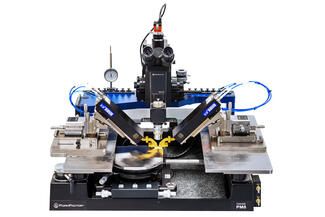
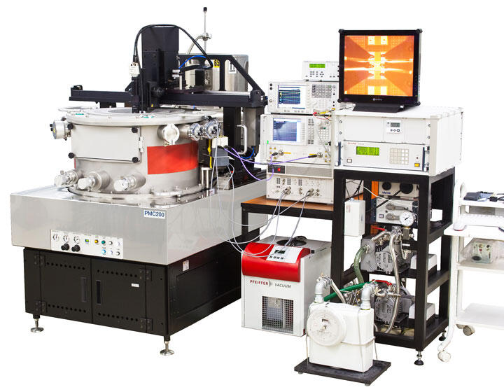
FormFactor - Cascade PMC200 - 200 mm manual cryogenic probe system
-
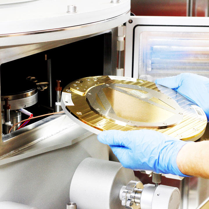
Different substrate carriers for wafers up to 200 mm or single dies
-
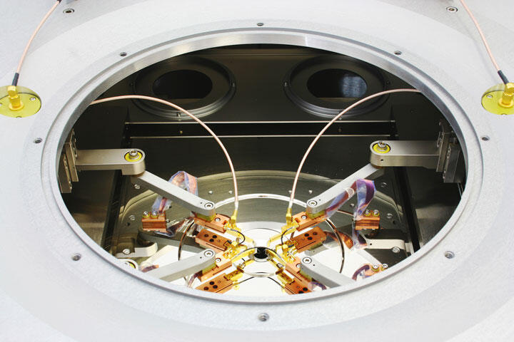
Probe cards and/or up to eight positioners
-
Independently cooled cold shield
-
Probe positioners placed inside vacuum chamber
-
Intuitive, manual drives
-
Front loading capability through load door
-
Independent control of linear chuck stage and positioners
-
Contact/separation stroke for chuck
Advanced manual cryogenic wafer probing < 7 K
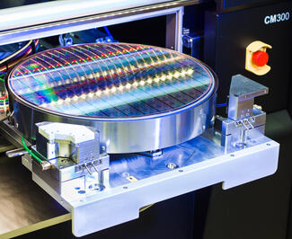
The PMC200 is a highly-precise, advanced manual probe system for wafers and substrates up to 200 mm in a high vacuum environment, at cryogenic temperatures down to 77 K with liquid nitrogen or < 7 K with liquid helium. Designed for educational and industrial environments, it supports a wide range of applications, including DC and RF measurements of the latest silicon, compound semiconductor and superconductor devices, MEMS and optoelectronic tests.
Applications
- IV/CV
- MEMS
- Opto
- RF/mmW/THz
Flexibility
- Different substrate carriers for wafers up to 200 mm or single dies
- Probe cards and/or up to eight positioners
- Use with liquid nitrogen or helium, depending on the target temperature
- Accessories available, such as black bodies and optical motion analysis tools
- Designed for industrial environments
- Covers wide range of measurements (I-V, C-V, RF, MEMS, OPTO)
Stability
- Independently cooled cold shield
- Probe positioners placed inside vacuum chamber
- Short and stable probe arms
- Solid station frame with built-in vibration-isolation
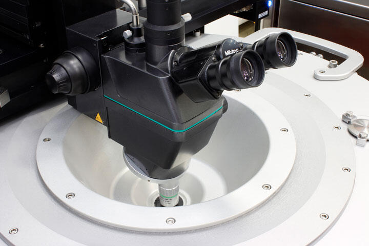
- Optional microscope bridge
- Optional upgrade for 300 mm wafer
- Ice- and condensation-free probing down to 77 K (liquid nitrogen) or below 7 K (liquid helium)
- Precise probe positioning
- Excellent measurement accuracy and repeatability
- Superior vibration attenuation
- Stable image quality for high-resolution microscopes
Ease of Use
- Intuitive, manual drives
- Front loading capability through load door
- Comfortable and easy operation
- Quick and ergonomic change of DUT
High measurement throughput
- Independent control of linear chuck stage and positioners
- Contact/separation stroke for chuck
- Fast, manual step-and-repeat testing of the whole wafer
- Simultaneous contacting and separation of all probes
More Product Information

-
Comprehensive I/O connections: Standard setup of up to 24 RF lines (up to 20 GHz) and 48 DC lines, with extensions to higher I/O connections possible.
-
Non-magnetic construction: Capable of characterizing qubits below 50 mK without magnetic interference when required.
-
Sample size: Proven with chips up to 10×10 mm in size.
-
Pressure-based contact: Connect test and measurement I/O to DUT pads using pressure only. No permanent connection required.

-
Wafer temp verified <4.5 K (with 44 RF probes in contact)
-
Magnetic field suppression to <200 nT
-
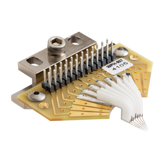
Easy exchange of customizable probe cards
-
Configurable for 150 mm, 200 mm and 300 mm wafers
-
Options for fully automated wafer load or manual
-
Complete software suite for manual, semi-auto, or fully automated probing
-
25 wafer cassette capacity for fully automated testing
-
~15 minute cooldown time per wafer

-
Ease of use – Less experienced operators can perform an RF calibration up to 500 GHz by simply pushing a button. This reduces the need of experienced users full time on each system.
-
Reduced Soak Time – The system will automatically re-align the probes to the pads if they drift from alignment. This reduces test time and increases throughput.
-
Unattended Use – Measurements can be left running over night or the weekend, testing all devices on the wafer, and at different temperatures without the need of an operator.
-
Calibration Monitor and Re-calibration – System will continuously monitor calibration drift, and automatically re-calibrate the system should the drift exceed a predefined limit.

-
Die-to-die stepping time of under 100 ms
-
Up to 20 dies/sec (70,000 dies/hour) with MultiDie Testing technology
-
Even extreme variations in height, such as the case with warped wafers, can be compensated
-
Interfaces to all major analysis instrumentation, optics software and testers
-
Access to top side and bottom side of device under test (DUT)
-
Highly accurate light measurement
-
Test automation out-of-cassette for 24/7 operation

-
Revolutionary technology advancement for wafer and die-level photonics probing
-
Real-time in-situ calibrations
-
Highest accuracy in test results
-
Lowest coupling loss
-
New innovative combination of hardware and software features to align and optimize fibers/arrays in a wafer-level trench
-
Minimized coupling losses with minimal trench dimensions
-
Industry standard for vertical coupling to wafer-level grating couplers
-
Dark, shielded and frost-free
-
-40°C to +125°C
-
Pioneering set of automated functions that perform critical calibrations of the optical positioning system to the probe station
-
Exclusive FormFactor-developed automated test methodology
-
FormFactor-developed graphical user interface to manually control the optical positioning system
-
Configurable between single fibers, fiber arrays and edge coupling holders

-
Different substrate carriers for wafers up to 150 mm or single dies
-
Up to six positioners
-
Probe positioners placed inside vacuum chamber
-
Short and stable probe arms
-
Ergonomic and straightforward design
-
Intuitive, manual operation
-
Independent control of linear chuck stage and positioners
-
Contact/separation stroke for probe platen

Customized Solutions for a Variety of Challenging Applications

-
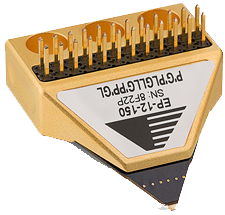
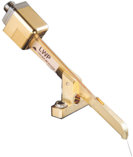
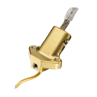
Combination of DC and RF in a single probe module: One dual probe or a maximum of three RF; a maximum of 9 DC standard (other quantities upon request).
-
Utilizes ACP tip design, GSG, GS or SG
-
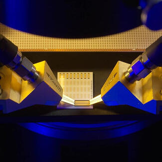
RF tips available from DC to 110 GHz
-
Choice of BeCu or tungsten tips
-
DC power needles come standard with 100 pF microwave capacitor
-
Power bypass inductance: 8 nH
-
Maximum DC voltage: 50 V without power bypassing (25 V with standard power bypassing, and component dependent with custom power bypassing)
-
Ideal for probing the entire circuit for functional test
-
Dual ACP configuration supports differential signaling applications
-
DC probes can provide power or slow logic to circuit under test

-
Quick and easy probe tip navigation
-
Z drive can work in the same range as the chuck
-
Enables higher separation gap while the DUT stays in focus
-
Automatically configure and optimize performance
-
24/7 operating
-
Increased MTBF
-
Protects the measurement setup
-
Prevents involuntary mechanical contact between lens and probes

FormFactor, Inc.
FormFactor, Inc. (NASDAQ:FORM) is a leading provider of essential test and measurement technologies along the full IC life cycle – from characterization, modeling, reliability, and design de-bug, to qualification and production test.
We constantly strive to help our customers solve the advanced test and measurement challenges of the broader semiconductor industry. Our focus on customer partnership, innovation, agility and operational excellence allows us to earn sustainable business every day.
Contact Details
FormFactor, Inc. Corporate Headquarters
7005 Southfront Road, Livermore, CA 94551, USA
Phone: 925-290-4000
Test & Measurement