Probe Systems
Products
-
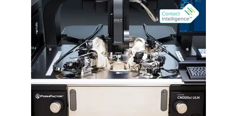
Ease of use – Less experienced operators can perform DC measurements by simply pushing a button. This reduces the need of experienced users full time on each system.
-
Reduced Soak Time – The system will automatically re-align the probes to the pads if they drift from alignment. This reduces test time and increases throughput.
-
Unattended Use – Measurements can be left running over night or the weekend, testing all devices on the wafer, and at different temperatures without the need of an operator.
-
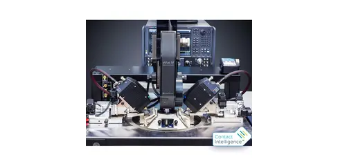
Ease of use – Less experienced operators can perform an RF calibration up to 500 GHz by simply pushing a button. This reduces the need of experienced users full time on each system.
-
Reduced Soak Time – The system will automatically re-align the probes to the pads if they drift from alignment. This reduces test time and increases throughput.
-
Unattended Use – Measurements can be left running over night or the weekend, testing all devices on the wafer, and at different temperatures without the need of an operator.
-
Calibration Monitor and Re-calibration – System will continuously monitor calibration drift, and automatically re-calibrate the system should the drift exceed a predefined limit.
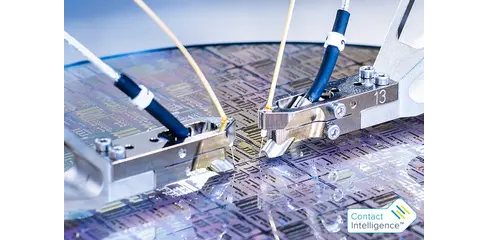
- Revolutionary technology advancement for wafer and die-level photonics probing
- Real-time in-situ calibrations
- Singulated die testing
- True die-level edge coupling
- In-situ power measurements
- Advanced calibration technologies
- Enables autonomous measurements
See "Specifications & Details" tab for more key features
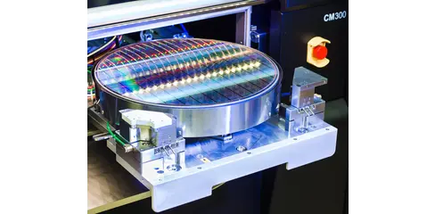
Flexibility
- Application flexibility: Coax, Triax, RF/mmW, High Power, Double Sided
- Temperatures range from -60°C to +300°C
- Surfaces are nickel or gold-plated
- Hybrid chuck design – operation with and without cooling unit
- Field-upgradeable: On-site cold upgrades for all main prober platforms
Highest Efficiency for Reduced Cost of Test
- Up to 25% lower air consumption (CDA) than other systems on the market with no compromise in transition times
- Up to 15% faster transition times than other systems on the market
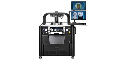
Flexibility
- DC, AC and RF/microwave device characterization, 1/f, WLR, FA and design debug
- Full thermal range of -60°C to +300°C
- Compatible with TopHat or IceShield
- Usage of manual and motorized positioners, probe cards within EMI-shielded environment
- Upgrade path to meet your future needs
- Stable and repeatable measurements over a wide thermal range
High accuracy and repeatability
- Reliable and repeatable contact
- Moisture-free, light-tight and EMI-shielded test environment with MicroChamber® technology
- Advanced EMI-shielding with PureLine and AttoGuard technologies available
- Superior low-leakage and low-noise measurements
- Safe and accurate hands-off testing
- Minimizes settling times for efficient measurements over full thermal range
See "Specifications & Details" tab for more key features
OptoVue
- Revolutionary technology advancement for wafer and die-level photonics probing
- Real-time in-situ calibrations
- Singulated die testing
- True die-level edge coupling
- In-situ power measurements
- Advanced calibration technologies
- Enables autonomous measurements
Horizontal Die-Level Edge Coupling
- Highest accuracy in test results
- Lowest coupling loss
- Repeatable measurement results due to exclusive automated fiber-to-facet alignment technology
- Reduced risk of damaging fibers with collision avoidance technology
- Ease of use for less experienced users
- Enables close simulation of real-world conditions with device performance closest to the final application
See "Specifications & Details" tab for more key features
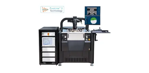
PureLine 3 Technology
- Provides an effectively noise free environment around the device under test (DUT)
- First automated probe station to achieve -190dB spectral noise*
- Up to 32x lower noise (1kHz), for improved device characterization and modelling at the 7/5/2 nm technology nodes targeted for 5G and beyond applications
- Eliminates over 97% of the environmental noise experienced in previous probe systems
- Extensive collection of FormFactor patents, electrical design knowledge, and measurement system IP
Plug In and Go
- World’s first probe station with integrated TestCell Power Management (a TestCell is a connected set of equipment, including test software, instruments, probe station, thermal system, and related measurement accessories such as cables and on-wafer probes)
- Eliminates all ground-loop induced TestCell noise
- Low field emissions
- Provides fully managed and filtered AC power to the entire system, prober and instruments
See "Specifications & Details" tab for more key features
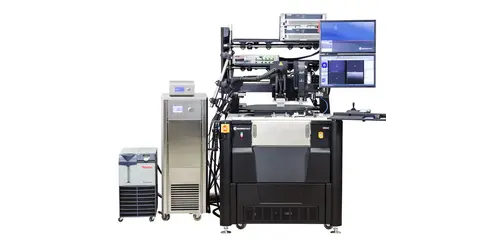
Customized Solutions for a Variety of Challenging Applications
We are your partner for challenging applications. Our comprehensive technical and application know-how over all probe system platforms and our expertise for customized products is based on an extensive experience over many years. We offer a special demo support in-house or at the customer, as well as after sales support for complicated setups.
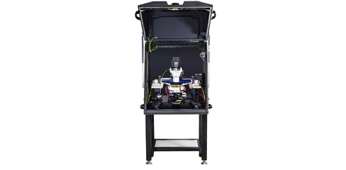
Optimized Measurement Setup
- Multi-purpose SIGMA instrument integration kit
- Shorter cabling and universal chuck connection
- Triax probe with protected guard
- Optimized signal path
- Safe probe tip exchange
- Seamless integration of various analyzers
High Power Chuck
- Triax design for low-leakage measurements up to 3 kV
- Special chuck surface coating
- High-isolation ready
- High-current measurement up to 100 A with lowest contact resistance
- Optional upgrade for 10 kV (coax) operating voltage
- Thin wafer handling capability
Safe Operation
- Arcing protection
- Shield Enclosure with interlock
- Advanced grounding concept
- Maximum protection from high-voltage shock for users and devices
- Common ground protection for all instruments
- EMI/light-tight shielded environment