FormFactor - Cascade PLC50 - 100 mm manual cryogenic probe system
-
Different substrate carriers for wafers up to 100 mm or single dies
-
Up to six positioners
-
Independently cooled cold shield
-
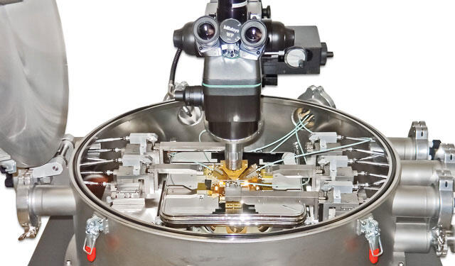
Probe positioners placed inside vacuum chamber
-
Ergonomic and straightforward design
-
Simple microscope operation
-
Independent control of linear chuck stage and positioners
-
Contact/separation stroke for probe platen
Entry-level manual cryogenic wafer probing < 7 K
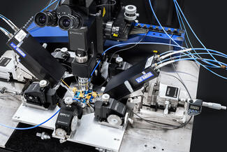
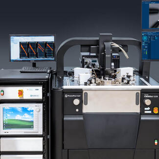
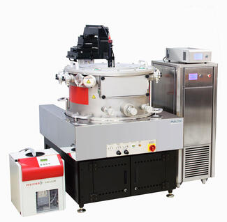
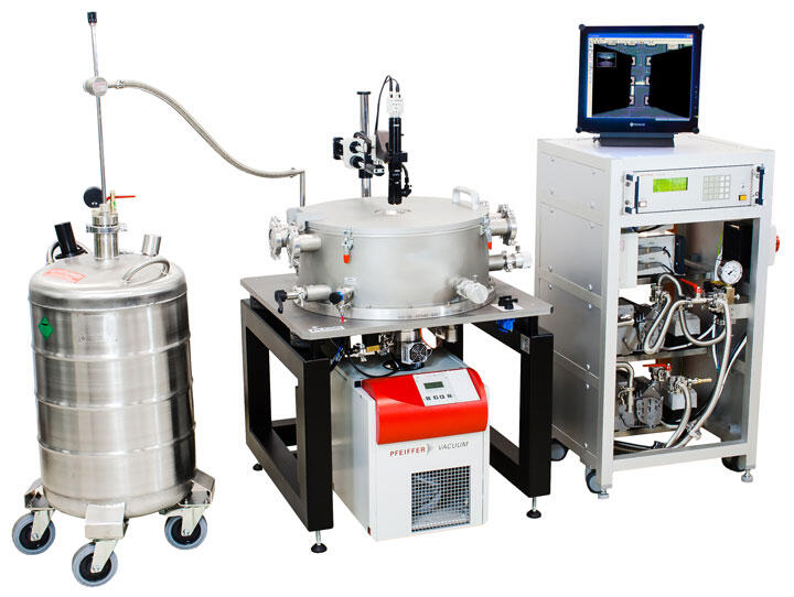
The PLC50 is a highly-precise, cost-effective probe station for wafers and substrates up to 100 mm in a high vacuum environment, at cryogenic temperatures down to 77 K with liquid nitrogen or < 7 K with liquid helium. Specially designed for laboratory requirements, it supports a wide range of applications, including DC and RF measurements of the latest silicon, compound semiconductor and superconductor devices, MEMS and optoelectronic tests.
Flexibility
- Different substrate carriers for wafers up to 100 mm or single dies
- Up to six positioners
- Use with liquid nitrogen or helium, depending on the target temperature
- Probing with an open chamber lid possible under atmospheric condition
- Specially designed for laboratory environments
- Covers wide range of measurements (I-V, C-V, RF, MEMS, OPTO)
Stability
- Independently cooled cold shield
- Probe positioners placed inside vacuum chamber
- Short and stable probe arms
- Solid station frame with built-in vibration-isolation
- Ice- and condensation-free probing down to 77 K (liquid nitrogen) or below 7 K (liquid helium)
- Precise probe positioning
- Excellent measurement accuracy and repeatability
- Superior vibration attenuation
Ease of Use
- Ergonomic and straightforward design
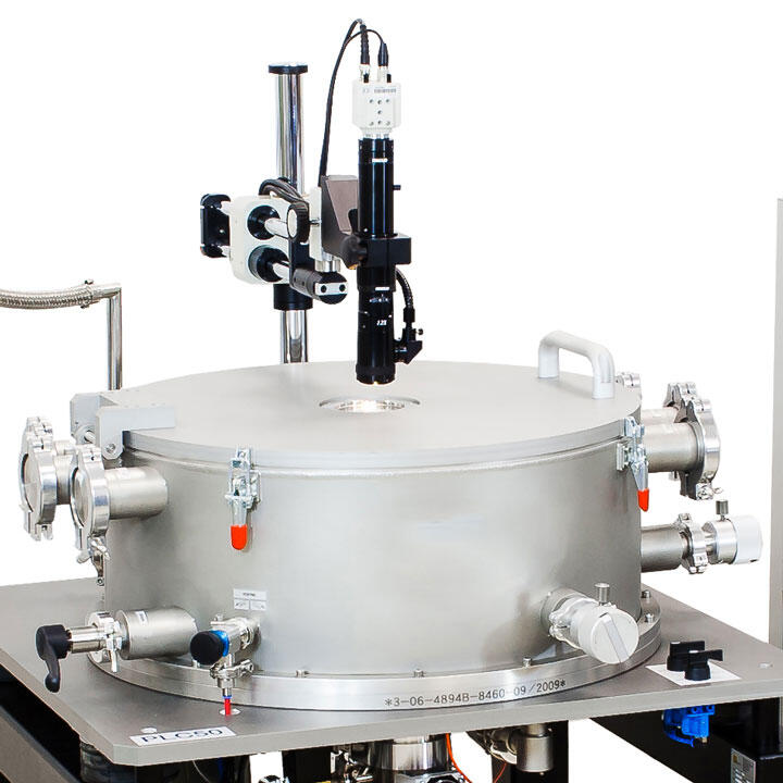
- Simple microscope operation
- Hinged topside lid
- Comfortable and easy operation
- Quick and ergonomic change of DUT
- Topside access to probes and samples
High measurement throughput
- Independent control of linear chuck stage and positioners
- Contact/separation stroke for probe platen
- Fast, manual step-and-repeat testing of the whole wafer
- Simultaneous contacting and separation of all probes
More Product Information
Customized Solutions for a Variety of Challenging Applications

-
Best price per contact – typically over one million (1,000,000) touchdowns
-
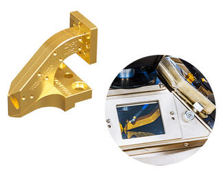
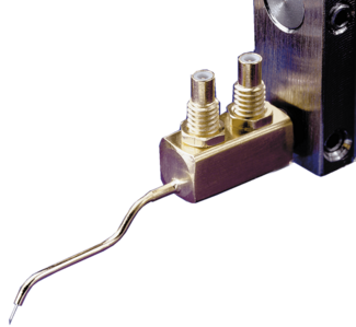
RF/Microwave signal is shielded and completely air isolated in the probe body
-
Excellent performance in vacuum environments and temperatures as low as 4 K, or as high as 300°C
-
Highest impedance control with perfectly-symmetrical, MEMS-machined coplanar contact structure
-
Probe on any pad material with minimal damage

-
Functional temperature range of -263 to +150°C
-
Stainless steel tip material for thermal decoupling
-
Coaxial cable with TCE matched inner and outer conductors
-
Consistent tip geometry even at cryogenic temperatures

-
Provides an effectively noise free environment around the device under test (DUT)
-
World’s first probe station with integrated TestCell Power Management (a TestCell is a connected set of equipment, including test software, instruments, probe station, thermal system, and related measurement accessories such as cables and on-wafer probes)
-
Up to 4x faster flicker noise thermal testing on 30 μm pads
-
Provides dark and dry environment for measuring light sensitive transistors, and devices at negative temperatures (<= -60°C) with frost free operation
-
Provides fully managed and filtered AC power to the entire system – prober and instruments
-
Filters harmful noise generated by external thermal control systems
-
Reduced “antenna effect” injection of unwanted RF noise into the measurement path
-
Provide up to 100dB attenuation (50Hz to 80Mhz) with 100mA max DC current handling
-
Ultra-low, fA-level current and fF-level capacitance measurements from -65 °C to + 300 °C
-
Enables full access to the chuck and the auxiliary sites
-
Intuitive, and precise movement of chuck in X, Y, and Z-direction
-
User-centered design minimizes training costs and enhances efficiency
-
Test automation out-of-cassette for higher test cell efficiency for over-night/over-weekend operation

-
Fully isolated experiment space for true 4K temperatures during probing
-
Cryogenic positioners to provide large travel ranges without warming up the device
-
Flexible thermal jumpers to ensure high thermal conductance and low mechanical transmission
-
A soft vacuum bellows provides a compliant mounting interface for the cryocooler
-
Quick release vacuum feedthroughs for easy configurability
-
A large rectangular port for high signal capacity

-
Wafer temp verified <4.5 K (with 44 RF probes in contact)
-
Magnetic field suppression to <200 nT
-
Easy exchange of customizable probe cards
-
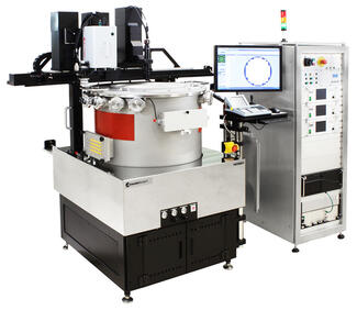
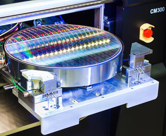
Configurable for 150 mm, 200 mm and 300 mm wafers
-
Options for fully automated wafer load or manual
-
Complete software suite for manual, semi-auto, or fully automated probing
-
25 wafer cassette capacity for fully automated testing
-
~15 minute cooldown time per wafer

-
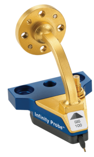
Infinity Probe: best for Al (Si)
-
ACP Probe: best for AU (III-Vs)
-
|Z| Probe: robust solution (long lifetime)
-
RF chuck ±3 μm surface planarity
-
Unique 500 μm platen contact/ separation stroke with ≤± 1 μm accuracy for repeatable contact
-
Exclusive 1-, 2-, 3-, and 4-port on-wafer calibration algorithms
-
Automated calibration monitoring

-
Replace costly and inflexible test fixtures with easy-to-use probe tips
-
Long lifetime – typically over 1,000,000 contacts
-
GS/SG footprint up to 4 GHz and GSG up to 20 GHz
-
High-power RF test: up to 30 Watts
-
Test at temperatures from -60°C to 200°C

-
Load-lock chamber: Cycle devices 10X faster in a cryogenic environment
-
High-density electrical interface at cryogenic temperatures: More pins on the device enables more test structures to be probed with a single cooldown
-
Base temperature of < 2K or < 4K with high cooling power: Test devices at the temperatures that matter most for pre- screening and evaluating device performance
-
Low vibration: Stable contact with the device under test and enables low noise measurements

FormFactor, Inc.
FormFactor, Inc. (NASDAQ:FORM) is a leading provider of essential test and measurement technologies along the full IC life cycle – from characterization, modeling, reliability, and design de-bug, to qualification and production test.
We constantly strive to help our customers solve the advanced test and measurement challenges of the broader semiconductor industry. Our focus on customer partnership, innovation, agility and operational excellence allows us to earn sustainable business every day.
Contact Details
FormFactor, Inc. Corporate Headquarters
7005 Southfront Road, Livermore, CA 94551, USA
Phone: 925-290-4000
Test & Measurement