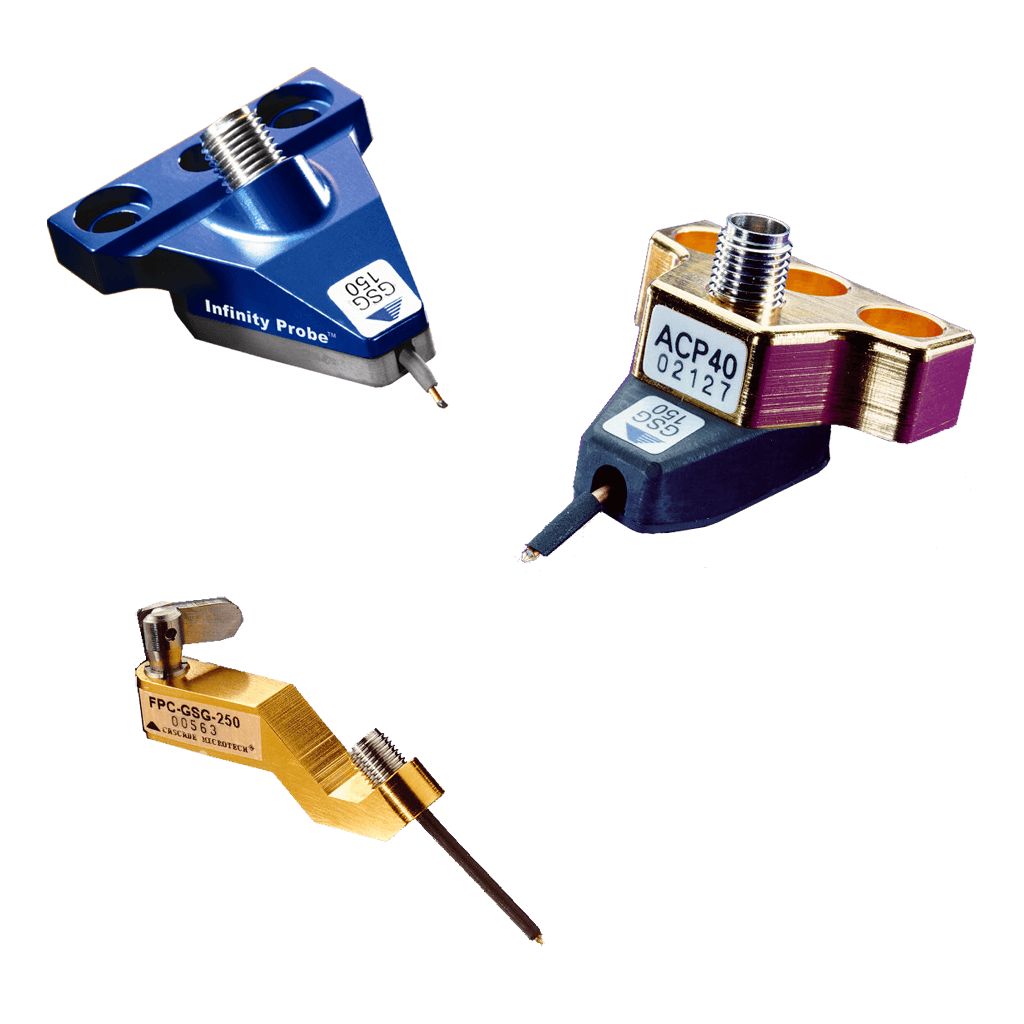
FormFactor - Cascade Resistive Matching and Termination - Custom configured for your application
- Choice of Series resistance or Termination (signal line to ground)
- Use of High Performance RF Resistors
- Choice of Resistor values available
- Choice of body styles, Infinity, ACP or FPC
- Can help to stabilize oscillations in high-gain devices
- Impedance match to low dynamic resistance laser diodes
- Custom configured for your application
Resistive Impedance Matching Probes and Termination probes are available for the following probe families: Infinity; ACP; FPC, in multiple configurations. We use high performance / high quality RF resistors for these Matching or Termination probes and the resistors are placed as close as possible to the tip/DUT, to minimize the path length between the DUT and the resistor. The available Resistance values are limited and are listed in the request form. These types of Impedance Matching and Termination probes are used in various application such as with laser diodes, Transmission Line Pulse, ensure better termination of 50 ohm test equipment when mated to high impedance devices, etc.
More Product Information
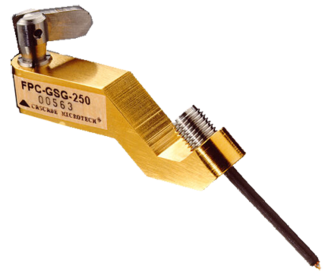
- DC-40 GHz bandwidth
- 10 ps rise time
- Low insertion and return loss
- 2 mils of tip-to-tip compliance
- High probing angle and clearance
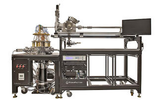
Cryogenic Temperatures
- Fully isolated experiment space for true 4K temperatures during probing
- Cryogenic positioners to provide large travel ranges without warming up the device
- Integrated helium pot for high temperature stability of the device under test
- Fully dry cryogen-free cooler eliminates the need for expensive helium circulation systems
- Rapid cool liquid nitrogen option for faster cool down times
See "Specifications & Details" tab for more key features
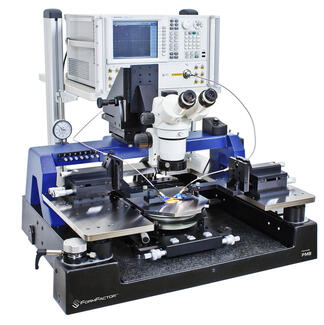
Three Probe Technologies
- Infinity Probe: best for Al (Si)
- ACP Probe: best for AU (III-Vs)
- |Z| Probe: robust solution (long lifetime)
- Precision contact on a wide variety of materials from 26 GHz to 67 GHz
- Accurate results with excellent crosstalk
- Matching cables and substrates included
Precise Contact Solution
- RF chuck ±3 μm surface planarity
- Unique 500 μm platen contact/ separation stroke with ≤± 1 μm accuracy for repeatable contact
- Precision probe alignment
- Consistent contact force and overtravel
- Stable contact performance
WinCal Calibration Software
- Exclusive 1-, 2-, 3-, and 4-port on-wafer calibration algorithms
- Automated calibration monitoring
- Unique measurement & analysis methods
- Accurate S-parameter measurements
- Automatic calibration setup for higher efficiency
- Fast and easy data interpretation and reporting
-
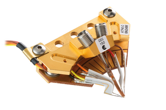
Combination of DC and RF in a single probe module: One dual probe or a maximum of three RF; a maximum of 9 DC standard (other quantities upon request).
-
Utilizes ACP tip design, GSG, GS or SG
-
RF tips available from DC to 110 GHz
-
Choice of BeCu or tungsten tips
-
DC power needles come standard with 100 pF microwave capacitor
-
Power bypass inductance: 8 nH
-
Maximum DC voltage: 50 V without power bypassing (25 V with standard power bypassing, and component dependent with custom power bypassing)
-
Ideal for probing the entire circuit for functional test
-
Dual ACP configuration supports differential signaling applications
-
DC probes can provide power or slow logic to circuit under test
Flexibility
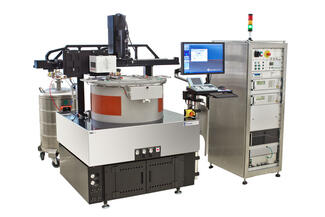
- Different substrate carriers for wafers up to 200 mm or single dies
- Probe cards and/or up to eight positioners
- Use with liquid nitrogen or helium, depending on the target temperature. Or use of cryo-cooler for dry-cooling option.
- Accessories available, such as black bodies and optical motion analysis tools
- Optional upgrade for 300 mm wafer
- Designed for industrial environments
- Covers wide range of measurements (I-V, C-V, RF, MEMS, OPTO)
- Ideal for small structures
See "Specifications & Details" tab for more key features
-
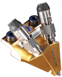
Best price per contact – typically over one million (1,000,000) touchdowns
-
RF/Microwave signal is shielded and completely air isolated in the probe body
-
Excellent performance in vacuum environments and temperatures as low as 4 K, or as high as 300°C
-
Highest impedance control with perfectly-symmetrical, MEMS-machined coplanar contact structure
-
Probe on any pad material with minimal damage
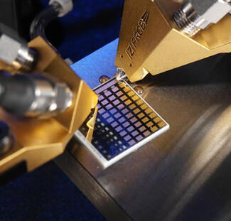
The CSR family of calibration substrates delivers the highest accuracy available due to the high quality of each substrate. The calibration standards are manufactured using rugged, hard gold, which ensures a long lifetime.
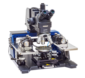
Flexibility
- Ideal for a wide range of applications such as RF, mm-Wave and sub-THz characterization, FA, DWC, MEMS, optoelectronic tests and WL
- Re-configurable and upgradable as requirements grow
- Minimizes setup times with no loss in performance or accuracy
- Seamless integration of various measurement instruments
Stability
- Solid station frame
- Built-in vibration-isolation solution for superior vibration attenuation
- Rigid microscope bridge
- Compact and rigid mechanical design
- Highly accurate measurement results
- Incorporates best-known methods
Ease of Use
- Ergonomic and straightforward design for comfortable and easy operation
- Low-profile design
- Simple microscope operation
- Quick and ergonomic change of DUT through pull-out stage
- Minimize training efforts
- Fast time to data
- Convenient operation
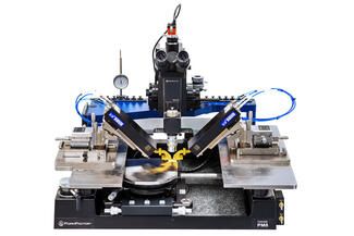
SlimVue Microscope
- Combined eye-pieces and CCD camera mount
- 3x zoom and quick lens exchange
- Quick lens exchange
- 1 um optical resolution
- Minimized scope footprint
- Fast change from navigation optics to high-resolution optics
- Resolving ‹ 50 μm pads
- Simple integration with any mmW modules
Application Specific Sigma Kits
- Engraved guides on mmW platen
- Supports broadband, load pull, coax RF and banded waveguide configuration
- Optical feedback on platen position (gauge)
- Adaptable to any mmW/sub-THz applications
- Seamless integration with any mmW modules and tuners
- Fast mounting and setup change
THz measurement capability
- Rock-solid mechanical design
- Submicron stage accuracy
- Optical feedback on platen and probe position (gauge)
- Motorized positioner
- <+-1 um separation repeatability
- Micrometer-accurate and repeatable probe placement and overtravel
- Highly-precise and stable THz measurements
FormFactor, Inc.
FormFactor, Inc. (NASDAQ:FORM) is a leading provider of essential test and measurement technologies along the full IC life cycle – from characterization, modeling, reliability, and design de-bug, to qualification and production test.
We constantly strive to help our customers solve the advanced test and measurement challenges of the broader semiconductor industry. Our focus on customer partnership, innovation, agility and operational excellence allows us to earn sustainable business every day.
