You design the future. We help you make it happen.
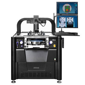
FormFactor - Cascade Ultra High-Power (UHP) - Enabling single-contact high-current/high-voltage test
- Enables coaxial measurements up to 10,000 V and 300 A pulsed (600 A in a parallel configuration) with a single touchdown
- Even distribution of high current with innovative multi-fingertip design
- Compatible with TESLA 200/300 mm power device characterization system
- Reduced measurement time by testing both high-voltage and high-current conditions with a single touchdown
- Accurate characterization of a wide range of pad sizes and test currents, with minimum pad damage and contact resistance
- Safe, reliable and repeatable high-current/voltage measurements over a wide temperature range (from -55°C to +300°C)
FormFactor’s Ultra-High-Power Probe (UHP), a high-voltage parametric probe, handles both high voltage (up to 10,000 V) and high current (up to 600 A) at a wide temperature range (-60ºC to 300ºC).
The high pulse current achieves full I-V characterization with one setup and one touchdown. Together with a TESLA on-wafer power device characterization system, the UHP fully utilizes the high-voltage/current capability of Keysight B1505A and N1265A Ultra High Current Expanders.
Document
Document
More Product Information

- Ultra-low, fA-level current and fF-level capacitance measurements from -65 °C to + 300 °C
- Guarantees fully-guarded measurements to fA and fF levels
- Individual connectors provide force-sense connection for quasi-Kelvin and CV measurements
- Allows probing of different pad materials and sizes
- Fast replacement of worn probes without the need for tools

- Accommodates a combination of up to four Cascade Microtech probes
- Configurable for mixed-signal RF/mmW testing
- Quick and easy repairs to be performed in the field, by simply replacing individual probes
- Adaptable to new device layouts by exchanging individual probes

- Light-tight version and EMI-shielded version for low noise and light-sensitive measurements
- Application flexibility, ideal for use in high frequency applications
- Sized to accommodate thermal chucks, laser cutter, and video equipment on the probe system
- Suitable for integration with vibration isolating tables

-
Replace costly and inflexible test fixtures with easy-to-use probe tips
-
Long lifetime – typically over 1,000,000 contacts
-
GS/SG footprint up to 4 GHz and GSG up to 20 GHz
-
High-power RF test: up to 30 Watts
-
Test at temperatures from -60°C to 200°C
Flexibility
- DC, AC and RF/microwave device characterization, 1/f, WLR, FA and design debug
- Full thermal range of -60°C to +300°C
- Compatible with TopHat or IceShield
- Usage of manual and motorized positioners, probe cards within EMI-shielded environment
- Upgrade path to meet your future needs
- Stable and repeatable measurements over a wide thermal range
High accuracy and repeatability
- Reliable and repeatable contact
- Moisture-free, light-tight and EMI-shielded test environment with MicroChamber® technology
- Advanced EMI-shielding with PureLine and AttoGuard technologies available
- Superior low-leakage and low-noise measurements
- Safe and accurate hands-off testing
- Minimizes settling times for efficient measurements over full thermal range
See "Specifications & Details" tab for more key features
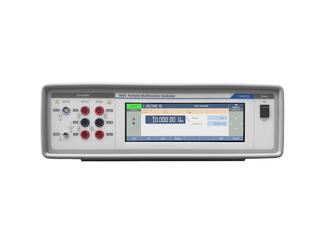
65 ppm AC/DC multifunction calibrator designed specifically for calibration of 3½ and 4½ digit multimeters. 1050 V, 20.5 A, resistance, capacitance and temperature packed inside ultra portable, 11 kg body.
- Compact, light, ideal for onsite calibrations
- 1050 V, 20.5 A, resistance, capacitance, TC, RTD and frequency
- Basic accuracy 60 ppm
- All-round calibrator for 3.5 and 4.5 digit multimeters

Flexibility
- Different substrate carriers for wafers up to 100 mm or single dies
- Up to six positioners
- Use with liquid nitrogen or helium, depending on the target temperature
- Probing with an open chamber lid possible under atmospheric condition
- Specially designed for laboratory environments
- Covers wide range of measurements (I-V, C-V, RF, MEMS, OPTO)
See "Specifications & Details" tab for more key features

Comprehensive, Turn-key Integrated Measurement System (IMS) with Keysight Photonics Application

Flexibility
- Different substrate carriers for wafers up to 200 mm or single dies
- Probe cards and/or up to eight positioners
- Optional thermal chuck (-60°C to 300°C) and pressure regulation
- Accessories available, such as black bodies and optical motion analysis tools
- Optional upgrade for 300 mm wafer
- Designed for industrial environments
- Covers wide range of measurements (I-V, C-V, RF, MEMS, OPTO)
- Ideal for small structures
See "Specifications & Details" tab for more key features
FormFactor, Inc.
Website
FormFactor, Inc. (NASDAQ:FORM) is a leading provider of essential test and measurement technologies along the full IC life cycle – from characterization, modeling, reliability, and design de-bug, to qualification and production test.
We constantly strive to help our customers solve the advanced test and measurement challenges of the broader semiconductor industry. Our focus on customer partnership, innovation, agility and operational excellence allows us to earn sustainable business every day.
 - Enabling single-contact high-current/high-voltage test")