You design the future. We help you make it happen.
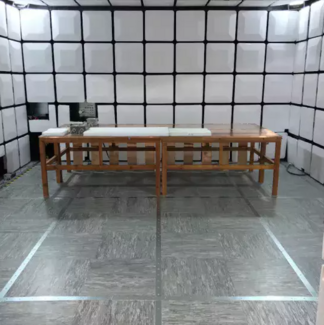
FormFactor - Cascade Shield Enclosure Light-tight probing
- Light-tight version and EMI-shielded version for low noise and light-sensitive measurements
- Application flexibility, ideal for use in high frequency applications
- Sized to accommodate thermal chucks, laser cutter, and video equipment on the probe system
- Suitable for integration with vibration isolating tables
Shield Enclosures are designed for durable stability and sized to accommodate analytical probers equipped with all kinds of accessories, including thermal chucks, laser cutters, TV and emission cameras. The EMI-shielded version guarantees a light-tight and electromagnetically shielded environment for all sensitive measurements.
More Product Information

- Power bypass inductance: 8 nH
- Standard DCQ probes have flat tip needles available in nickel-plated tungsten or BeCu with diameters of 0.75 mil, 1.0 mil and 1.5 mil.
- Supports collinear and non-standard needle configurations
- Up to 16 DC for standard; maximum of 24 DC for custom
- Ideal for probing the entire circuit for functional test
- DC probes can provide power or slow logic to circuit under test

- On-Off power switch
- 20 A Circuit Breaker
- 8’ Flexible Power Cord
- Outlets – (4) 5-20R
Test Tap:
- 3ft.
- (2) fork terminals (current)
- (1) fork terminals (ground)
- (2) Shielded Banana (voltage)

Flexibility
- Application flexibility: Coax, Triax, RF/mmW, High Power, Double Sided
- Temperatures range from -60°C to +300°C
- Surfaces are nickel or gold-plated
- Hybrid chuck design – operation with and without cooling unit
- Field-upgradeable: On-site cold upgrades for all main prober platforms
Highest Efficiency for Reduced Cost of Test
- Up to 25% lower air consumption (CDA) than other systems on the market with no compromise in transition times
- Up to 15% faster transition times than other systems on the market

Comprehensive, Turn-key Integrated Measurement System (IMS) with Keysight SPA for On-wafer DC Parametric Measurements

High flexibility
- Re-configurable for DC, RF, mmW, FA, WLR and more
- Thermal range: -60˚C to 300˚C available
- Upgrade path to meet your future needs
- Stable and repeatable measurements over a wide thermal range
See "Specifications & Details" tab for more key features

SlimVue Microscope
- Combined eye-pieces and CCD camera mount
- 3x zoom and quick lens exchange
- Quick lens exchange
- 1 um optical resolution
- Minimized scope footprint
- Fast change from navigation optics to high-resolution optics
- Resolving ‹ 50 μm pads
- Simple integration with any mmW modules
Application Specific Sigma Kits
- Engraved guides on mmW platen
- Supports broadband, load pull, coax RF and banded waveguide configuration
- Optical feedback on platen position (gauge)
- Adaptable to any mmW/sub-THz applications
- Seamless integration with any mmW modules and tuners
- Fast mounting and setup change
THz measurement capability
- Rock-solid mechanical design
- Submicron stage accuracy
- Optical feedback on platen and probe position (gauge)
- Motorized positioner
- <+-1 um separation repeatability
- Micrometer-accurate and repeatable probe placement and overtravel
- Highly-precise and stable THz measurements
A high performance RF-shielded EMC chamber specifically designed for emc measurements in accordance with MIL-STD-461E/F and RTCA DO160 requirements.

- Lithographic thin-film construction
- Excellent crosstalk characteristics
- Non-oxidizing nickel alloy tips
- Innovative force delivery mechanism
- 40GHz, 50GHz, 67GHz, 110GHz and 145GHz connectors available
- GSG, SG, GS, GSGSG, GSSG, SGS configurations
- 50 to 250 µm pitches (other pitches available on request)
- High current version (2 A) available
Advantages
- Superior field confinement reduces unwanted couplings to nearby devices and transmission modes
- Superior measurement accuracy and repeatability
- Small scrub minimizes damage to aluminum pad
- Typical contact resistance < 0. 05 Ω on Al, <0.02Ω on Au
- Save valuable wafer space and reduce pad parasitics by being able to shrink pad geometries to 25 x 35 µ m (best case)

- Coaxial and triaxial measurements up to 10,000 V
- High-quality construction with low-noise electrical performance
- Replaceable probe tips in a variety of tip sizes
- Temperature range of of -60°C to 300°C
- Triaxial measurement ensures a much better understanding of device leakage in the off state
- Highly reliable, stable and repeatable measurements
- Integrally designed as part of a complete measurement solution
FormFactor, Inc.
Website
FormFactor, Inc. (NASDAQ:FORM) is a leading provider of essential test and measurement technologies along the full IC life cycle – from characterization, modeling, reliability, and design de-bug, to qualification and production test.
We constantly strive to help our customers solve the advanced test and measurement challenges of the broader semiconductor industry. Our focus on customer partnership, innovation, agility and operational excellence allows us to earn sustainable business every day.
