You design the future. We help you make it happen.
FormFactor - Cascade Vibration Isolation Tables - Tables from simple to highly sensitive
- Designed for use with specific Probe Systems
- Tables to suit all facility requirements and applications
- Stable probing, even in submicron range
- Granite platen ensures rigidity and temperature stability
- Can be combined with the Shield Enclosures
Full range of vibration isolation tables
Working with increasingly small scales of reference means that any vibration however minimal, even from the equipment itself, will seriously degrade a probe station’s performance. Slight vibrations will cause the probes to jump and miss their contacts and the microscope image will be blurred. Our range of vibration isolation tables includes a simple table for general working conditions as well as specifically designed tables for very sensitive measurements such as in the submicron range.
Document
More Product Information
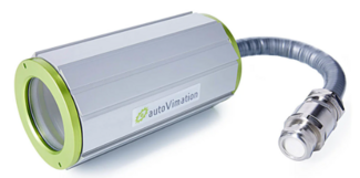
- For cameras up to 61 x 61mm cross section
- Perfect for underwater use
- IP68 protection class
- Double seal system
- Robust construction
- Flexible camera positioning
- High chemical resistance
- Vibration‐proof mounting
- Camera mount included
- Excellent heat dissipation
- Integration of ring lights possible
- Tested 12h in 10m water depth

- Light-tight version and EMI-shielded version for low noise and light-sensitive measurements
- Application flexibility, ideal for use in high frequency applications
- Sized to accommodate thermal chucks, laser cutter, and video equipment on the probe system
- Suitable for integration with vibration isolating tables

DC, RF and Optical Probe Positioning for Highest Accuracy Measurements
FormFactor offers a wide variety of manual and motorized probe positioners for any application from DC to terahertz measurements and beyond.
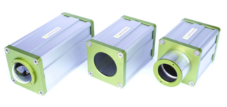
- For cameras up to 100 x 100mm cross section
- 3" or 4" window for large diameter lenses
- Integrated water cooling channels option
- Vibration‐proof mounting
- Flexible camera positioning
- Excellent heat dissipation
- With flange:
- Suitable for Meganova ring light
- all Orca lids and extensions usable
- High IP protection class and chemical resistance
- For cameras up to 40 x 40mm cross section
- Front tube for easy lens access
- Robust construction
- Compact size
- High IP protection class
- Flexible camera positioning
- High chemical resistance
- Vibration‐proof mounting
- Camera mount included
- Excellent heat dissipation

Three Probe Technologies
- Infinity Probe: best for Al (Si)
- ACP Probe: best for AU (III-Vs)
- |Z| Probe: robust solution (long lifetime)
- Precision contact on a wide variety of materials from 26 GHz to 67 GHz
- Accurate results with excellent crosstalk
- Matching cables and substrates included
Precise Contact Solution
- RF chuck ±3 μm surface planarity
- Unique 500 μm platen contact/ separation stroke with ≤± 1 μm accuracy for repeatable contact
- Precision probe alignment
- Consistent contact force and overtravel
- Stable contact performance
WinCal Calibration Software
- Exclusive 1-, 2-, 3-, and 4-port on-wafer calibration algorithms
- Automated calibration monitoring
- Unique measurement & analysis methods
- Accurate S-parameter measurements
- Automatic calibration setup for higher efficiency
- Fast and easy data interpretation and reporting

Flexibility
- Different substrate carriers for wafers up to 200 mm or single dies
- Probe cards and/or up to eight positioners
- Use with liquid nitrogen or helium, depending on the target temperature
- Accessories available, such as black bodies and optical motion analysis tools
- Designed for industrial environments
- Covers wide range of measurements (I-V, C-V, RF, MEMS, OPTO)
See "Specifications & Details" tab for more key features

- Revolutionary technology advancement for wafer and die-level photonics probing
- Real-time in-situ calibrations
- Singulated die testing
- True die-level edge coupling
- In-situ power measurements
- Advanced calibration technologies
- Enables autonomous measurements
See "Specifications & Details" tab for more key features

Environmental Control
- Wafer temp verified <4.5 K (with 44 RF probes in contact)
- Magnetic field suppression to <200 nT
- Highly uniform wafer temperature
- Precise thermal stability and control
- Solid construction with granite base enables precision motion and vibration control
See "Specifications & Details" tab for more key features
FormFactor, Inc.
Website
FormFactor, Inc. (NASDAQ:FORM) is a leading provider of essential test and measurement technologies along the full IC life cycle – from characterization, modeling, reliability, and design de-bug, to qualification and production test.
We constantly strive to help our customers solve the advanced test and measurement challenges of the broader semiconductor industry. Our focus on customer partnership, innovation, agility and operational excellence allows us to earn sustainable business every day.
