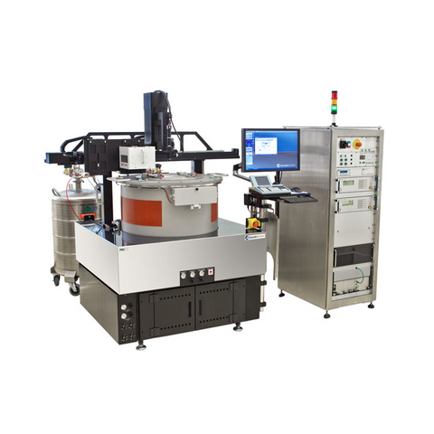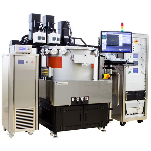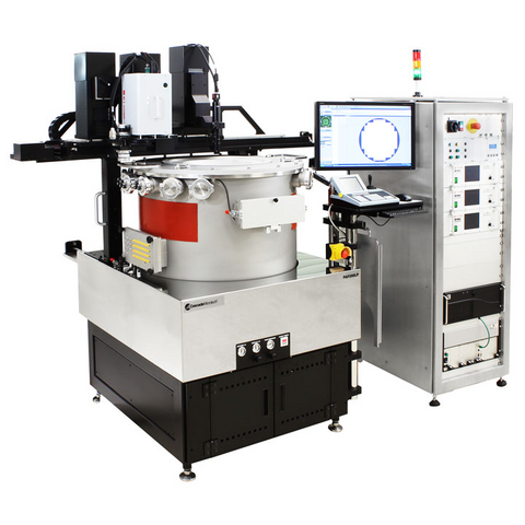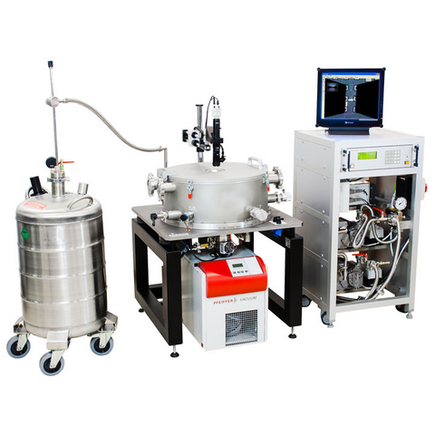

FormFactor, Inc. (NASDAQ:FORM) is a leading provider of essential test and measurement technologies along the full IC life cycle – from characterization, modeling, reliability, and design de-bug, to qualification and production test.
We constantly strive to help our customers solve the advanced test and measurement challenges of the broader semiconductor industry. Our focus on customer partnership, innovation, agility and operational excellence allows us to earn sustainable business every day.
Contact Details
FormFactor, Inc. Corporate Headquarters
7005 Southfront Road, Livermore, CA 94551, USA
Phone: 925-290-4000
Test & Measurement
Products
Flexibility
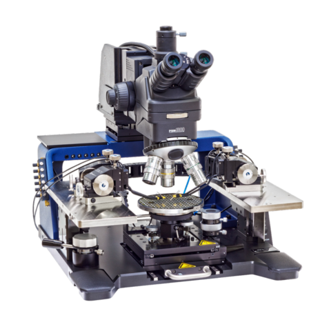
- Ideal for a wide range of applications such as RF, mm-Wave and sub-THz characterization, FA, DWC, MEMS, optoelectronic tests and WL
- Re-configurable and upgradable as requirements grow
- Minimizes setup times with no loss in performance or accuracy
- Seamless integration of various measurement instruments
Stability
- Solid station frame
- Built-in vibration-isolation solution for superior vibration attenuation
- Rigid microscope bridge
- Compact and rigid mechanical design
- Highly accurate measurement results
- Incorporates best-known methods
Ease of Use
- Ergonomic and straightforward design for comfortable and easy operation
- Low-profile design
- Simple microscope operation
- Quick and ergonomic change of DUT through pull-out stage
- Minimize training efforts
- Fast time to data
- Convenient operation
- Ideal for multiport RF/Microwave and high-speed digital signal testing
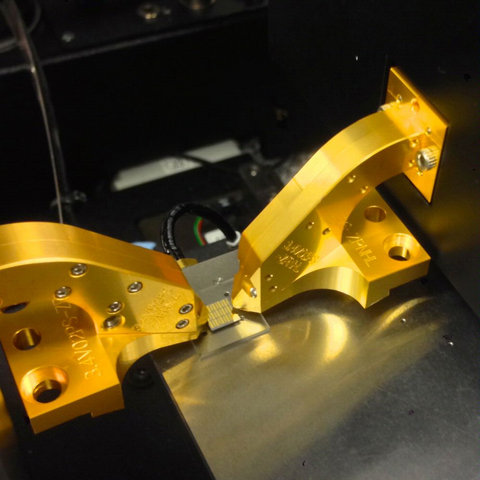
- Mix DC and RF/Microwave signals on one probe
- Long lifetime – typically over one million (1,000,000) touchdowns
- Excellent performance in temperatures ranging from 10 K to 200°C
- Probe on any pad material with no damage
- Substrate material: High-resistivity silicon
- Substrate thickness: 275 µm
- Dielectric constant: 11.8
- Nominal Z0: 50 Ω
-
Die-to-die stepping time of under 100 ms
-
Up to 20 dies/sec (70,000 dies/hour) with MultiDie Testing technology
-
Even extreme variations in height, such as the case with warped wafers, can be compensated
-
Interfaces to all major analysis instrumentation, optics software and testers
-
Access to top side and bottom side of device under test (DUT)
-
Highly accurate light measurement
-
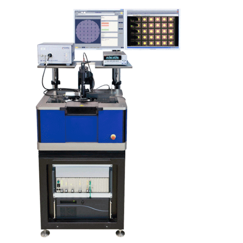
Test automation out-of-cassette for 24/7 operation
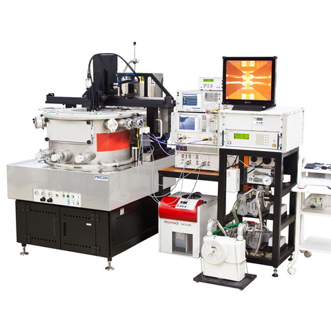
Flexibility
- Different substrate carriers for wafers up to 200 mm or single dies
- Probe cards and/or up to eight positioners
- Use with liquid nitrogen or helium, depending on the target temperature. Or use of cryo-cooler for dry-cooling option.
- Accessories available, such as black bodies and optical motion analysis tools
- Optional upgrade for 300 mm wafer
- Designed for industrial environments
- Covers wide range of measurements (I-V, C-V, RF, MEMS, OPTO)
- Ideal for small structures
See "Specifications & Details" tab for more key features
Flexibility
- Different substrate carriers for wafers up to 200 mm or single dies
- Probe cards and/or up to eight positioners
- Optional thermal chuck (-60°C to 300°C) and pressure regulation
- Accessories available, such as black bodies and optical motion analysis tools
- Optional upgrade for 300 mm wafer
- Designed for industrial environments
- Covers wide range of measurements (I-V, C-V, RF, MEMS, OPTO)
- Ideal for small structures
See "Specifications & Details" tab for more key features
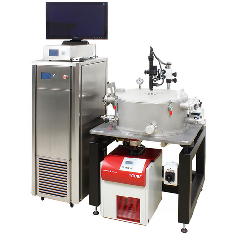
Flexibility
- Different substrate carriers for wafers up to 100 mm or single dies
- Up to six positioners
- Use with liquid nitrogen or helium, depending on the target temperature
- Probing with an open chamber lid possible under atmospheric condition
- Specially designed for laboratory environments
- Covers wide range of measurements (I-V, C-V, RF, MEMS, OPTO)
See "Specifications & Details" tab for more key features
Flexibility
- Different substrate carriers for wafers up to 150 mm or single dies
- Up to six positioners
- Optional thermal chuck (-60°C to 300°C) and pressure regulation
- Probing with an open chamber lid possible under atmospheric condition
- Specially designed for laboratory environments
- Covers wide range of measurements (I-V, C-V, RF, MEMS, OPTO)
See "Specifications & Details" tab for more key features
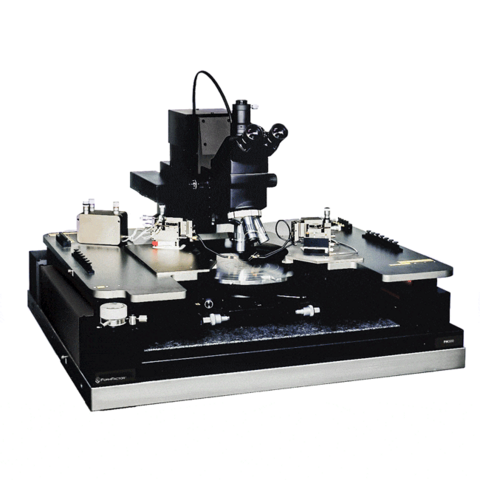
Superior Mechanics
- Highly stable granite base
- Independent, coarse movement of X and Y axes, combined with easy fine adjustments
- Excellent measurement accuracy and repeatability
- Fast navigation and high-precision probe positioning
See "Specifications & Details" tab for more key features
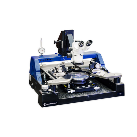
Superior Mechanics
- Highly stable granite base
- Independent, coarse movement of X and Y axes, combined with easy fine adjustments down to submicron ranges
- 1 µm repeatable separation stroke
- Excellent measurement accuracy and repeatability
- Fast navigation and high-precision probe positioning
See "Specifications & Details" tab for more key features
Flexibility
- Different substrate carriers for wafers up to 200 mm or single dies
- Probe cards and/or up to eight positioners
- Use with liquid nitrogen or helium, depending on the target temperature
- Accessories available, such as black bodies and optical motion analysis tools
- Designed for industrial environments
- Covers wide range of measurements (I-V, C-V, RF, MEMS, OPTO)
See "Specifications & Details" tab for more key features
