
FormFactor, Inc. (NASDAQ:FORM) is a leading provider of essential test and measurement technologies along the full IC life cycle – from characterization, modeling, reliability, and design de-bug, to qualification and production test.
We constantly strive to help our customers solve the advanced test and measurement challenges of the broader semiconductor industry. Our focus on customer partnership, innovation, agility and operational excellence allows us to earn sustainable business every day.
Contact Details
FormFactor, Inc. Corporate Headquarters
7005 Southfront Road, Livermore, CA 94551, USA
Phone: 925-290-4000
Test & Measurement
Products
Floating Action Buttons
- Easy and fast setup of camera views
- Go to Light and Image Settings of the selected camera view with only one mouse click
Workflow Wizard
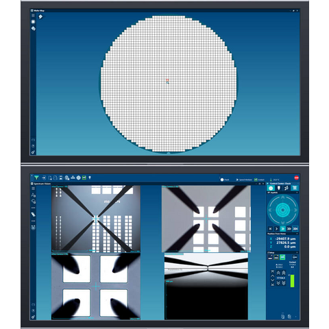
- Guided workflows for wafer setups, alignment tools and Autonomous Assistants
- Workflow wizard shows task-relevant settings and options only
- Wizard settings can be corrected anytime – no need to restart the wizard
- Wizard helps with intelligent solutions in case of error
See "Specifications & Details" tab for more key features
- Designed for use with specific Probe Systems
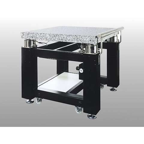
- Tables to suit all facility requirements and applications
- Stable probing, even in submicron range
- Granite platen ensures rigidity and temperature stability
- Can be combined with the Shield Enclosures
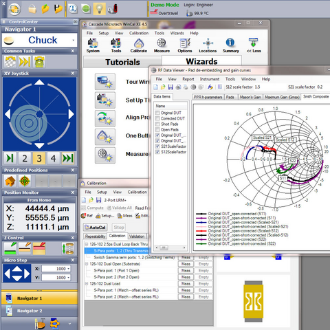
More than a calibration tool
- Calibration
- Validation
- Measurement
- Analysis
No one supports more VNA’s
- Support of more than 24 of the most common VNA’s
Tool for the novice
- Guided wizards and multimedia tutorials integrated
- Intelligence in setups
See "Specifications & Details" tab for more key features
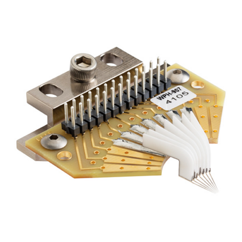
- Full-radius, nickel-plated tungsten needles
- Power bypass inductance: 16 nH
- Supports collinear and non-standard needle configurations
- Support up to a maximum of 12 ceramic blades DC needles / contacts
- Ideal for probing the entire circuit for functional test
- DC probes can provide power or slow logic to circuit under test
Cryogenic Temperatures
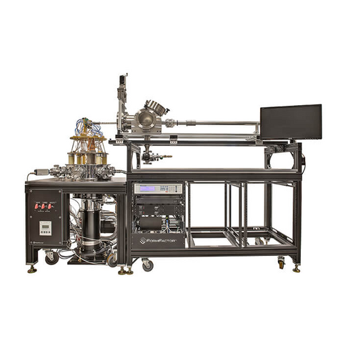
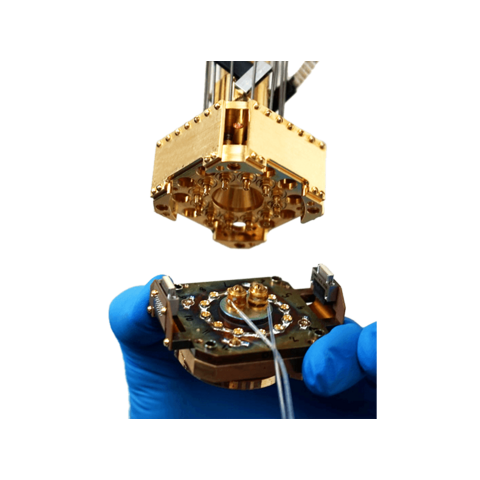
- Fully isolated experiment space for true 4K temperatures during probing
- Cryogenic positioners to provide large travel ranges without warming up the device
- Integrated helium pot for high temperature stability of the device under test
- Fully dry cryogen-free cooler eliminates the need for expensive helium circulation systems
- Rapid cool liquid nitrogen option for faster cool down times
See "Specifications & Details" tab for more key features
Environmental Control
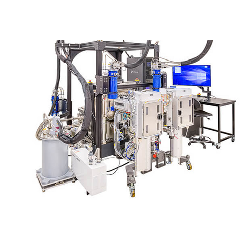
- Wafer temp verified <4.5 K (with 44 RF probes in contact)
- Magnetic field suppression to <200 nT
- Highly uniform wafer temperature
- Precise thermal stability and control
- Solid construction with granite base enables precision motion and vibration control
See "Specifications & Details" tab for more key features
- Tests and validates performance directly on silicon without post-dicing packaging
- Dramatically reduces time to data and shortens development cycles
- Enables high scalability for high volume manufacturing
- Offers flexibility in chip design with full grid probing
