You design the future. We help you make it happen.
FormFactor - Cascade Positioners - DC, RF and optical probe positioning for highest accuracy measurements
DC, RF and Optical Probe Positioning for Highest Accuracy Measurements
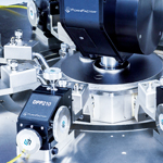
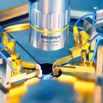
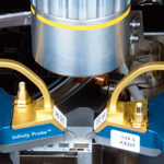
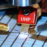
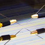
FormFactor offers a wide variety of manual and motorized probe positioners for any application from DC to terahertz measurements and beyond.
Engineered for high stability and accuracy, FormFactor‘s positioners enable precise, backlash-free and repeatable probe tip placements – from simple IV/CV measurements to highly challenging measurement tasks.
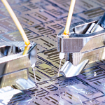
Enhanced with FormFactor‘s High Temperature Stability (HTS), the positioners become part of our exclusive Contact Intelligence™ Technology that enables small pad probing over a full temperature range.
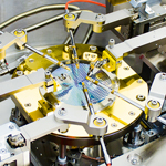
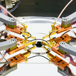
Unsurpassed accuracy and highest productivity is achieved with the revolutionary Autonomous Measurement Assistants for DC, RF and Silicon Photonics testing. These wafer probing assistants utilize our programmable positioners and enable fully autonomous, hands-free measurements – minimizing training needs and accelerating time to market.
Designed and validated with proven quality standards, our positioners are always the perfect match to your FormFactor probe station.
Application Flexibility
|
|
|
|
|
|
|
|
|
|
Probe Station Compatibility
|
MPS150 / EPS150 |
Summit |
PM8 / EPS200 |
CM300xi |
PA300 / PM300 |
Tesla |
Vac / Cryo |
|
|---|---|---|---|---|---|---|---|
|
Manual Positioners |
|||||||
|
DPP105 |
O |
- |
O | X |
O |
X |
X |
|
DPP2xx |
O |
O |
O |
O |
O |
O |
X |
|
DPP3xx |
O |
- |
O |
- |
O |
- |
X |
|
DPP450 |
O |
- |
- |
- |
- |
X |
X |
|
VCP110 |
X |
X |
X |
X |
X |
X |
O |
|
RPP210 |
O |
O |
O |
O |
O |
O |
X |
|
RPP304 |
O |
O |
O |
O |
X |
X |
X |
|
RPP305 |
O |
- |
O |
O |
O |
X |
X |
|
RPP404 |
O |
O |
O |
O |
X |
X |
X |
|
rmmWLAP |
X |
O |
O |
O |
- |
- |
X |
|
Motorized Positioners |
|||||||
|---|---|---|---|---|---|---|---|
|
RPP504 |
X |
O |
O |
O |
X |
X |
X |
|
PH510 |
X |
X |
O |
- |
O |
X |
X |
|
SiPh |
X |
O2 |
X |
O |
X |
X |
X |
|
O Recommended |
| - Possible (not recommended) | |
X Not Compatible |
|
1Summit2000 only |
||
|
2Summit200 only |
More Product Information

Flexibility
- Application flexibility: Coax, Triax, RF/mmW, High Power, Double Sided
- Temperatures range from -60°C to +300°C
- Surfaces are nickel or gold-plated
- Hybrid chuck design – operation with and without cooling unit
- Field-upgradeable: On-site cold upgrades for all main prober platforms
Highest Efficiency for Reduced Cost of Test
- Up to 25% lower air consumption (CDA) than other systems on the market with no compromise in transition times
- Up to 15% faster transition times than other systems on the market

OptoVue
- Revolutionary technology advancement for wafer and die-level photonics probing
- Real-time in-situ calibrations
- Singulated die testing
- True die-level edge coupling
- In-situ power measurements
- Advanced calibration technologies
- Enables autonomous measurements
Horizontal Die-Level Edge Coupling
- Highest accuracy in test results
- Lowest coupling loss
- Repeatable measurement results due to exclusive automated fiber-to-facet alignment technology
- Reduced risk of damaging fibers with collision avoidance technology
- Ease of use for less experienced users
- Enables close simulation of real-world conditions with device performance closest to the final application
See "Specifications & Details" tab for more key features

- Light-tight version and EMI-shielded version for low noise and light-sensitive measurements
- Application flexibility, ideal for use in high frequency applications
- Sized to accommodate thermal chucks, laser cutter, and video equipment on the probe system
- Suitable for integration with vibration isolating tables

Comprehensive, Turn-key Integrated Measurement System (IMS) with Keysight Photonics Application

- Power bypass inductance: 8 nH
- Standard DCQ probes have flat tip needles available in nickel-plated tungsten or BeCu with diameters of 0.75 mil, 1.0 mil and 1.5 mil.
- Supports collinear and non-standard needle configurations
- Up to 16 DC for standard; maximum of 24 DC for custom
- Ideal for probing the entire circuit for functional test
- DC probes can provide power or slow logic to circuit under test

High-voltage/current Probes
- On-wafer power device characterization up to 10,000 V DC / 600 A
- Reduced probe and device destruction at high currents up to 20 A DC and 300 A pulse
- Increased isolation resistance and dielectric strength to provide full triaxial capability at high voltage (3,000 V) for low-leakage measurement

- DC-40 GHz bandwidth
- 10 ps rise time
- Low insertion and return loss
- 2 mils of tip-to-tip compliance
- High probing angle and clearance

PureLine 3 Technology
- Provides an effectively noise free environment around the device under test (DUT)
- First automated probe station to achieve -190dB spectral noise*
- Up to 32x lower noise (1kHz), for improved device characterization and modelling at the 7/5/2 nm technology nodes targeted for 5G and beyond applications
- Eliminates over 97% of the environmental noise experienced in previous probe systems
- Extensive collection of FormFactor patents, electrical design knowledge, and measurement system IP
Plug In and Go
- World’s first probe station with integrated TestCell Power Management (a TestCell is a connected set of equipment, including test software, instruments, probe station, thermal system, and related measurement accessories such as cables and on-wafer probes)
- Eliminates all ground-loop induced TestCell noise
- Low field emissions
- Provides fully managed and filtered AC power to the entire system, prober and instruments
See "Specifications & Details" tab for more key features

- Ideal for multiport RF/Microwave and high-speed digital signal testing
- Mix DC and RF/Microwave signals on one probe
- Long lifetime – typically over one million (1,000,000) touchdowns
- Excellent performance in temperatures ranging from 10 K to 200°C
- Probe on any pad material with no damage
FormFactor, Inc.
Website
FormFactor, Inc. (NASDAQ:FORM) is a leading provider of essential test and measurement technologies along the full IC life cycle – from characterization, modeling, reliability, and design de-bug, to qualification and production test.
We constantly strive to help our customers solve the advanced test and measurement challenges of the broader semiconductor industry. Our focus on customer partnership, innovation, agility and operational excellence allows us to earn sustainable business every day.


