You design the future. We help you make it happen.
Teledyne LeCroy - Probe Adapters
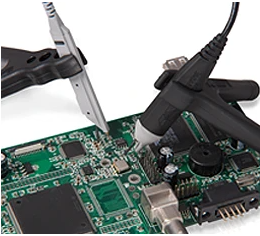
Probe adapters provide simple and easy interface of third-party probes as well as change between the different Teledyne LeCroy Oscilloscope input and cable types (ProBus, ProLink, K/2.92 mm, BNC and SMA). Depending on the adapters, changing between the Teledyne LeCroy Oscilloscope's input type may have an effect on the overall performance of the channel.
|
Products |
|
|---|---|
|
TekProbe to ProBus Probe Adapter |
|
|
ProLink to 2.92mm Adapter with Probe Power and Communication Pass Through |
|
|
ProLink to 2.92mm ProAxial Adapter with Probe Power and Communication Pass Through |
|
|
2.92mm to ProBus Adapter with Probe Power and Communication Pass Through |
|
|
2.92mm to ProLink Adapter with Probe Power and Communication Pass Through |
|
Document
Document
More Product Information

-
Functional temperature range of -263 to +150°C
-
Stainless steel tip material for thermal decoupling
-
Coaxial cable with TCE matched inner and outer conductors
-
Consistent tip geometry even at cryogenic temperatures

- Up to 12 contacts; any contact can be DC, Power, Logic to 500 MHz,or RF to 20 GHz
- Online design configuration tool helps you to specify your probe in minutes
- All designs are fully quadrant compatible
- Full solution includes probes, calibration substrates, stations, accessories and software
- Scalable architecture for future needs

- Coaxial and triaxial measurements up to 10,000 V
- High-quality construction with low-noise electrical performance
- Replaceable probe tips in a variety of tip sizes
- Temperature range of of -60°C to 300°C
- Triaxial measurement ensures a much better understanding of device leakage in the off state
- Highly reliable, stable and repeatable measurements
- Integrally designed as part of a complete measurement solution

Superior Mechanics
- Highly stable granite base
- Independent, coarse movement of X and Y axes, combined with easy fine adjustments down to submicron ranges
- 1 µm repeatable separation stroke
- Excellent measurement accuracy and repeatability
- Fast navigation and high-precision probe positioning
See "Specifications & Details" tab for more key features

- Vector Network Analyzer Frequency Range from 10 MHz up to 3.2 GHz
- Spectrum Analyzer Frequency Range from 9 kHz up to 3.2 GHz
- -156 dBm/Hz Displayed Average Noise Level (Typ.)
- -98 dBc/Hz @10 kHz Offset Phase Noise (1 GHz, Typ.)
- Total Amplitude Accuracy < 1.2 dB
- 1 Hz Minimum Resolution Bandwidth (RBW)
- All-Digital IF Technology
- Standard Preamplifier
- Distance to fault capability using VNA time domain analysis
- Up to 1.5 GHz Tracking Generator Kit
- Built-in Advanced Measurement capability (CHP, ACPR, OBW, CNR, TOI, etc)
- 10.1 lnch WVGA (1024 x 600) Display
The ZS Series probes provide high impedance and an extensive set of probe tips and ground accessories to handle a wide range of probing scenarios. The high 1 MΩ input resistance and low 0.9 pF input capacitance means this probe is ideal for all frequencies. The ZS Series probes provide full system bandwidth with all Teledyne LeCroy oscilloscopes with bandwidths of 4 GHz and lower.

DC, RF and Optical Probe Positioning for Highest Accuracy Measurements
FormFactor offers a wide variety of manual and motorized probe positioners for any application from DC to terahertz measurements and beyond.

-
Combination of DC and RF in a single probe module: One dual probe or a maximum of three RF; a maximum of 9 DC standard (other quantities upon request).
-
Utilizes ACP tip design, GSG, GS or SG
-
RF tips available from DC to 110 GHz
-
Choice of BeCu or tungsten tips
-
DC power needles come standard with 100 pF microwave capacitor
-
Power bypass inductance: 8 nH
-
Maximum DC voltage: 50 V without power bypassing (25 V with standard power bypassing, and component dependent with custom power bypassing)
-
Ideal for probing the entire circuit for functional test
-
Dual ACP configuration supports differential signaling applications
-
DC probes can provide power or slow logic to circuit under test

Flexibility
- Different substrate carriers for wafers up to 100 mm or single dies
- Up to six positioners
- Use with liquid nitrogen or helium, depending on the target temperature
- Probing with an open chamber lid possible under atmospheric condition
- Specially designed for laboratory environments
- Covers wide range of measurements (I-V, C-V, RF, MEMS, OPTO)
See "Specifications & Details" tab for more key features
Teledyne LeCroy
Website
12bit MSO's 40 Mhz to 100 GHz, Probes, Series Network & Logic Analyzers
