
You design the future. We help you make it happen.
Products
Displaying 289 - 300 of 804
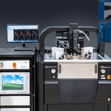
Comprehensive, Turn-key Integrated Measurement System (IMS) with Keysight A-LFNA for On-wafer R&D Advanced Low-Frequency Noise Measurements
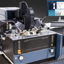
Comprehensive, Turn-key Integrated Measurement System (IMS) with Keysight PNA for On-wafer R&D Measurements from RF to millimeter wave to Terahertz
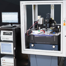
Comprehensive, Turn-key Integrated Measurement System (IMS) with Keysight PDA for On-wafer R&D Power Semiconductor Device Characterization Measurements
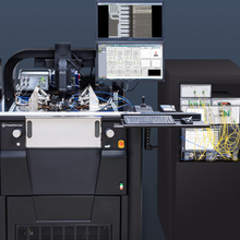
Comprehensive, Turn-key Integrated Measurement System (IMS) with Keysight Photonics Application
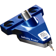
Lithographic thin-film construction
Excellent crosstalk characteristics
Non-oxidizing nickel alloy tips
Innovative force delivery mechanism
40GHz, 50GHz, 67GHz, 110GHz and 145GHz connectors available
GSG, SG, GS, GSGSG, GSSG, SGS configurations
50 to 250 µm pitches (other pitches available on request)
High current version (2 A) available
Advantages
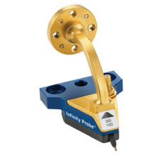
Probe loss is 3 dB typical between 140 and 200 GHz, S11/S22 15 dB typical
Reduced unwanted couplings and transmission modes
Able to shrink pad geometries to 25 x 35 µm (best case)
Typical contact resistance < 0.05 Ω on Al, < 0.02 Ω on Au
WR15, WR12, WR10, WR8, WR6, WR4, WR3, and WR2 bands available.
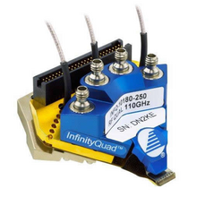
Customizable configuration up to 25 contacts: RF, Eye-Pass power, ground, logic
Lithographically-defined tips allow automated over temperature measurement on pads as small as 30 µm x 50 µm
Low and repeatable contact resistance on aluminum pads (< 0.05 Ω) ensures accurate results
Durable probe structure ensures more than 250,000 contacts
Able to measure from -40°C to +125°C without compromising performance or accuracy of specifications
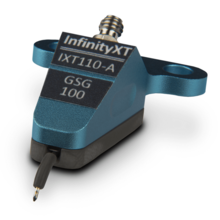
Next Generation Wafer Probing
Continues the Infinity family’s Industry leading electrical performance
High temperature capability (175° C +) for automotive device characterization and other applications
Better tip visibility for enhanced placement accuracy and repeatability
Improved tip life/durability with solid rhodium contacts
New tip architecture enables support for narrower pitches (e.g. 25um)
Advanced mechanical design combined with small contacts enables probing on smaller pads/pitches and improves durability and robustness
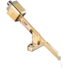
The LWP series Lightwave Probe enables optical measurements for on-wafer and hybrid photonics devices. It features user replaceable fiber pigtails allowing the probe to be optimized for a variety of light delivery and light collection applications including the characterization of topside illuminated photodiodes, Vertical Cavity Surface Emitting Lasers (VCSELs), hybrid transmitters and receivers, and LEDs.
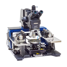
Flexibility
Ideal for a wide range of applications such as RF, mm-Wave and sub-THz characterization, FA, DWC, MEMS, optoelectronic tests and WL
Re-configurable and upgradable as requirements grow
Minimizes setup times with no loss in performance or accuracy
Seamless integration of various measurement instruments
Stability
Solid station frame
Built-in vibration-isolation solution for superior vibration attenuation
Rigid microscope bridge
Compact and rigid mechanical design
Highly accurate measurement results
Incorporates best-known methods
Ease of Use
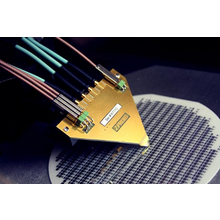
Ideal for multiport RF/Microwave and high-speed digital signal testing
Mix DC and RF/Microwave signals on one probe
Long lifetime – typically over one million (1,000,000) touchdowns
Excellent performance in temperatures ranging from 10 K to 200°C
Probe on any pad material with no damage
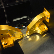
Substrate material: High-resistivity silicon
Substrate thickness: 275 µm
Dielectric constant: 11.8
Nominal Z0: 50 Ω