Products
Displaying 13 - 24 of 38
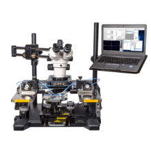
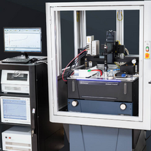
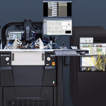
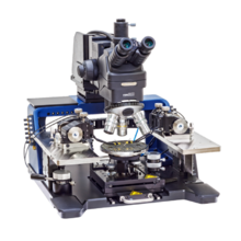
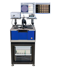
Probe station
Keysight Streamline Vector Network Analyzer (option up to 53 GHz)
Choice of probes
Known measurement accuracy traced back to independent standards
Comprehensive, Turn-key Integrated Measurement System (IMS) with Keysight SPA for On-wafer DC Parametric Measurements
Comprehensive, Turn-key Integrated Measurement System (IMS) with Keysight A-LFNA for On-wafer R&D Advanced Low-Frequency Noise Measurements
Comprehensive, Turn-key Integrated Measurement System (IMS) with Keysight PNA for On-wafer R&D Measurements from RF to millimeter wave to Terahertz
Comprehensive, Turn-key Integrated Measurement System (IMS) with Keysight PDA for On-wafer R&D Power Semiconductor Device Characterization Measurements
Comprehensive, Turn-key Integrated Measurement System (IMS) with Keysight Photonics Application
Ideal for a wide range of applications such as RF, mm-Wave and sub-THz characterization, FA, DWC, MEMS, optoelectronic tests and WL
Re-configurable and upgradable as requirements grow
Minimizes setup times with no loss in performance or accuracy
Die-to-die stepping time of under 100 ms
Up to 20 dies/sec (70,000 dies/hour) with MultiDie Testing technology
Even extreme variations in height, such as the case with warped wafers, can be compensated
Different substrate carriers for wafers up to 200 mm or single dies
Probe cards and/or up to eight positioners
Ice- and condensation-free probing down to 77 K (liquid nitrogen) or below 20 K (liquid helium)
Different substrate carriers for wafers up to 200 mm or single dies
Probe cards and/or up to eight positioners
Probe positioners placed inside vacuum chamber
Short and stable probe arms
Different substrate carriers for wafers up to 200 mm or single dies
Probe cards and/or up to eight positioners
Probe positioners placed inside vacuum chamber
Short and stable probe arms
Different substrate carriers for wafers up to 100 mm or single dies
Up to six positioners
Independently cooled cold shield
Probe positioners placed inside vacuum chamber
